Friday, October 19th 2012

AMD Third-Generation APUs to be Built on 28 nm Process
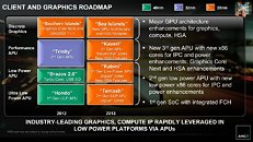
A leaked company roadmap slide revealed that AMD's third-generation performance APU, codenamed "Kaveri," will be built on the 28 nm silicon fabrication process. The chips will be built by Global Foundries. Kaveri combines AMD's next-generation CPU architecture codenamed "Steamroller" with Graphics CoreNext GPU architecture.
In addition to Kaveri, AMD will introduce a major update to its low-power APU lineup with "Kabini." A true successor to "Brazos," Kabini features x86-64 cores built on the energy-optimized "Jaguar" architecture (which succeeds "Bobcat," on which Brazos APUs are built). It is also mentioned that Kabini will be a true system-on-chip (SoC), with integration of the FCH chipset into the APU silicon. Such an integration could increase die size and complexity, but could also minimize the board footprint of the platform, making it possible to use the SoC in thin tablets, and COMs.In addition to the two, AMD touched on its ultra low power APU, codename "Temash." Like Kabini, Temash is a single-chip SoC, but extremely power optimized (we're talking about TDP numbers under 5W), making the chip optimized to compact tablets, and who knows, smartphones? Lastly, there's a mention of AMD's next-generation "Sea Islands" GPU architecture. AMD is promising "major GPU architecture enhancements," and confirmed that the new chips will be built on 28 nm process.
Source:
MyDrivers
In addition to Kaveri, AMD will introduce a major update to its low-power APU lineup with "Kabini." A true successor to "Brazos," Kabini features x86-64 cores built on the energy-optimized "Jaguar" architecture (which succeeds "Bobcat," on which Brazos APUs are built). It is also mentioned that Kabini will be a true system-on-chip (SoC), with integration of the FCH chipset into the APU silicon. Such an integration could increase die size and complexity, but could also minimize the board footprint of the platform, making it possible to use the SoC in thin tablets, and COMs.In addition to the two, AMD touched on its ultra low power APU, codename "Temash." Like Kabini, Temash is a single-chip SoC, but extremely power optimized (we're talking about TDP numbers under 5W), making the chip optimized to compact tablets, and who knows, smartphones? Lastly, there's a mention of AMD's next-generation "Sea Islands" GPU architecture. AMD is promising "major GPU architecture enhancements," and confirmed that the new chips will be built on 28 nm process.

25 Comments on AMD Third-Generation APUs to be Built on 28 nm Process
when is the price cut on the FM2 chips?
Given that low power chips are just being sampled now, you might be able to extrapolate time to market for the APU's.
phx.corporate-ir.net/External.File?item=UGFyZW50SUQ9MTI1MTM5fENoaWxkSUQ9LTF8VHlwZT0z&t=1
phx.corporate-ir.net/External.File?item=UGFyZW50SUQ9MTI1Mjk1fENoaWxkSUQ9LTF8VHlwZT0z&t=1
ir.amd.com/phoenix.zhtml?c=74093&p=irol-2012analystday
AMD Roadmaps
Lisa Su (page 20)
Closing at $2.18I would suggest that at least one sector isn't buying into the strategy