Monday, July 3rd 2017

AMD Readies Radeon Pro WX 9100: Vega for Professionals

After releasing the Vega Frontier Edition, AMD's take on a "prosumer" GPU which straddles the line between a professional and gaming graphics card, with somewhat mixed results, AMD is apparently now working on the fully professional version of the Vega silicon. Identified as the Radeon Pro WX 9100 (which is in line with AMD's current professional nomenclature), this professional graphics card will look to fully accelerate professional workloads, with a driver specifically crafted for such.

Recently rearing its head on CompuBench, the GPU features a low 1200 MHz clock speed, which is around 402 MHz lower than the Frontier Edition, and supposedly lower still than the Gaming RX Vega variant of the GPU. The Vega-based WX 9100 joins the Polaris-based WX 7100, WX 5100 and WX 4100 professional graphics cards, thus apparently topping out AMD's professional line-up for the year.
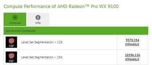
Source: Videocardz
Add your own comment

33 Comments on AMD Readies Radeon Pro WX 9100: Vega for Professionals

#26
Shihab
Umm, am I the only one who thinks this "playtest the game you're making on the same machine" thing is just marketing BS? Last time I checked, workstations cards can run games, and before you say but they don't run it as fast as gaming cards, I doubt devs optimise their games on >$500 cards, and if they wanted the fastest possible performance, there are much better options out there that can provide performance similar to what would actually be running in consumers' boxes!
the54thvoidSame card, different drivers.

Whoo.
The Pro will probably have ECC memory. A mandatory thing to be a true professional hardware, afaik.
Posted on Reply
#27
Vayra86
theoneandonlymrkWont happen Navi is going to be 7nm ,so we're not on 14nm that long.
This is wishful thinking more than anything else, and I'll tell you right now: not happening.

7nm hasn't even reached the market yet and 14nm was postponed for more than two years, after that we had one year of 16nm GPUs that costed an arm and a leg. 14nm is here to stay for awhile, at least 3-4 generations of GPU.

About this VEGA positioning... this is AMD spotting a market where the rest of the world never knew it was there. And in a couple years time, the numbers will underline the fact that the world never cared.
Posted on Reply
#28
TheoneandonlyMrK
Vayra86This is wishful thinking more than anything else, and I'll tell you right now: not happening.

7nm hasn't even reached the market yet and 14nm was postponed for more than two years, after that we had one year of 16nm GPUs that costed an arm and a leg. 14nm is here to stay for awhile, at least 3-4 generations of GPU.

About this VEGA positioning... this is AMD spotting a market where the rest of the world never knew it was there. And in a couple years time, the numbers will underline the fact that the world never cared.
7nm is on Gfs roadmap for 2h 2018 about the time an educated guess would have Navi on a frontier edition.
Mines based on facts and announcements mate your going by history and hearsay.
And whats Nvidia using 16nm got todo with anything Amd didn't.
Posted on Reply
#29
Vayra86
theoneandonlymrk7nm is on Gfs roadmap for 2h 2018 about the time an educated guess would have Navi on a frontier edition.
Mines based on facts and announcements mate your going by history and hearsay.
And whats Nvidia using 16nm got todo with anything Amd didn't.
History repeats, and in semiconductor business, every repeat is documented in the ever longer adoption time of a new node, because of the ever increasing issues that pop up to keep things running properly.

14nm was also announced for half a decade before it finally came to market, and when it did, the mobile space consumed stocks for a long long time.

Read back these comments in 2h 2018 and you'll nod in agreement. There is only one reason for all these announcements, and that is the need for investors and the creation of momentum to drive the adoption of the smaller node. Its strikingly similar to the 12901515181 announcements about the next best battery technology that never came, to secure budgets.
Posted on Reply
#30
TheoneandonlyMrK
Vayra86History repeats, and in semiconductor business, every repeat is documented in the ever longer adoption time of a new node, because of the ever increasing issues that pop up to keep things running properly.

14nm was also announced for half a decade before it finally came to market, and when it did, the mobile space consumed stocks for a long long time.

Read back these comments in 2h 2018 and you'll nod in agreement. There is only one reason for all these announcements, and that is the need for investors and the creation of momentum to drive the adoption of the smaller node. Its strikingly similar to the 12901515181 announcements about the next best battery technology that never came, to secure budgets.
Surprisingly know all that ,i was here watching too , before 28nm there were regular node swaps done easily ,the jump down to 14nm was harder than the jump to 7Nm will be and 7Nm is already at risk production status ,i think your guess is wrong and my guess is right.
Did i say it better for you that way.
And no these announcement coincide with both plans and design schedules, a chip takes years to design for a specific node so even if the node isnt fully ready designs are made to fit its expected specs.
Posted on Reply
#31
Vayra86
theoneandonlymrkSurprisingly know all that ,i was here watching too , before 28nm there were regular node swaps done easily ,the jump down to 14nm was harder than the jump to 7Nm will be and 7Nm is already at risk production status ,i think your guess is wrong and my guess is right.
Did i say it better for you that way.
And no these announcement coincide with both plans and design schedules, a chip takes years to design for a specific node so even if the node isnt fully ready designs are made to fit its expected specs.
I do agree it looks more concrete and hopeful than the wording used before 14nm launched, but on the other hand, when you read critically into this;

"Case in point, Samsung currently hopes to use EUV lithography for critical layers with their 7 nm nodes to avoid triple/quadruple patterning, but are being very careful in how they're wording their plans, saying that they are "reviewing possibilities" of EUV insertion at 7 nm. So it is not cast in stone that Samsung will not proceed with a DUV-only 7 nm if it has to. Meanwhile Intel also once considered to start using EUV for 7 nm. Finally, TSMC does not seem to be afraid of multi-patterning and intends to produce semiconductors using DUV-only 7 nm manufacturing tech in 2H 2018."
source: anandtech

Also, this;
www.semiwiki.com/forum/content/6631-euv-not-ready-7nm.html

We're actually talking about highly costly DUV lithography because EUV simply isn't good to go yet. In other words, everyone is at the stage where they know they can do 7nm, but the biggest hurdle will be economical of nature. A full DUV process will make the chip very expensive., much more so than the current node. The design phase is underway. But that is all she wrote... It seems highly likely that we'll see affordable consumer-7nm much later than 2018.
Posted on Reply
#32
TheoneandonlyMrK
Vayra86I do agree it looks more concrete and hopeful than the wording used before 14nm launched, but on the other hand, when you read critically into this;

"Case in point, Samsung currently hopes to use EUV lithography for critical layers with their 7 nm nodes to avoid triple/quadruple patterning, but are being very careful in how they're wording their plans, saying that they are "reviewing possibilities" of EUV insertion at 7 nm. So it is not cast in stone that Samsung will not proceed with a DUV-only 7 nm if it has to. Meanwhile Intel also once considered to start using EUV for 7 nm. Finally, TSMC does not seem to be afraid of multi-patterning and intends to produce semiconductors using DUV-only 7 nm manufacturing tech in 2H 2018."
source: anandtech

Also, this;
www.semiwiki.com/forum/content/6631-euv-not-ready-7nm.html

We're actually talking about highly costly DUV lithography because EUV simply isn't good to go yet. In other words, everyone is at the stage where they know they can do 7nm, but the biggest hurdle will be economical of nature. A full DUV process will make the chip very expensive., much more so than the current node. The design phase is underway. But that is all she wrote... It seems highly likely that we'll see affordable consumer-7nm much later than 2018.
So you agree 7Nm is already doable just uneconomical , euv is very far along but maybe not quite ready , i don't think foundries are dependent on euv for mass production of 7nm it is likely just going to take the right design to make it work ,a good example being small power efficient mobile chips , small as in small asic footprint.
Worthy of note though and tied , Amd is likely to also beat Nvidia to an McM chip with Navi.
Lots of small gpus on an interposer with next generation memory not hbm.
This approach could make an expensive process workable for Gpus.
Posted on Reply
#33
Vayra86
theoneandonlymrkSo you agree 7Nm is already doable just uneconomical , euv is very far along but maybe not quite ready , i don't think foundries are dependent on euv for mass production of 7nm it is likely just going to take the right design to make it work ,a good example being small power efficient mobile chips , small as in small asic footprint.
Worthy of note though and tied , Amd is likely to also beat Nvidia to an McM chip with Navi.
Lots of small gpus on an interposer with next generation memory not hbm.
This approach could make an expensive process workable for Gpus.
Its always like that with a new node, everything depends on good yields. I think our only difference here is that I'm more of a pessimist in this than you are :D
Posted on Reply
Add your own comment
Nov 22nd, 2024 02:27 EST change timezone

New Forum Posts

Popular Reviews

Controversial News Posts