Wednesday, January 14th 2009

AMD Justifies Use of Large L3 Cache on Phenom II, Opteron
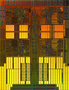
AMD's introduction of the Phenom II series processors served several purposes and goals for the company, mainly porting the processor technology to the newer 45nm SOI manufacturing node, to attempt to bring down manufacturing cost. This also meant that AMD could trade-off bringing down manufacturing cost with stepping up transistor counts on a die that is nearly the size of that of the 65nm Barcelona/Agena. The 45nm Shanghai/Deneb has a distinct feature over its predecessor: three times the amount of L3 cache. The larger cache significantly adds to the transistor count of the die: 758 million as against the 468 million on Barcelona/Agena. Replying to an inquiry of Hardware-Infos, AMD attempts to explain its motive behind incorporating the large L3 cache, while trading-off with savings of die-size and alleged latencies the L3 cache brings in.
AMD points out that expanding the L3 cache was important to the architecture in more ways than one. On the desktop/client PC front, the additional L3 cache was expected to provide a 5% performance increment over its predecessor. The reviews later backed AMD's assertion. Secondly, AMD likes to maintain an essentially common die design for both its client (Phenom II/Deneb) and enterprise or server (Opteron/Shanghai), to make sure manufacturing costs aren't wasted in setting up a separate manufacturing node. With the enterprise-grade Opteron processors, the 6 MB L3 cache has proven to benefit the processor in dealing with large server workloads. Finally, AMD claims that despite the larger cache, the overall die-area of the 45nm die remains lesser than that of the 65nm Stars die, so cost-cutting remains to an extant.
Source:
Hardware-Infos
AMD points out that expanding the L3 cache was important to the architecture in more ways than one. On the desktop/client PC front, the additional L3 cache was expected to provide a 5% performance increment over its predecessor. The reviews later backed AMD's assertion. Secondly, AMD likes to maintain an essentially common die design for both its client (Phenom II/Deneb) and enterprise or server (Opteron/Shanghai), to make sure manufacturing costs aren't wasted in setting up a separate manufacturing node. With the enterprise-grade Opteron processors, the 6 MB L3 cache has proven to benefit the processor in dealing with large server workloads. Finally, AMD claims that despite the larger cache, the overall die-area of the 45nm die remains lesser than that of the 65nm Stars die, so cost-cutting remains to an extant.

28 Comments on AMD Justifies Use of Large L3 Cache on Phenom II, Opteron
I didnt see much if any performance gain with DDR2 over DDR so thats why i kept with my old machine, and far as i can tell the faster the ram is the more you can overclock ya cpu? thats all i can tell that makes it worth wile...o and also its super cheap.
Id love to do up a skt A beast with a 3200+ and good ram and a 3850, it be sweet :D
I would of like to have seen AMD put alot of L2 cache on there new CPU's instead of L3 as my bro also says its just for show, but maybe not? it helped out C2D alot....