
2
Cores
2
Threads
15 W
TDP
2.9 GHz
Frequency
3.5 GHz
Boost
Stoney Ridge
Codename
Socket FP4
Socket

AMD Socket FP4
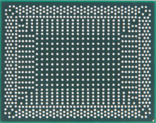
The AMD A9-9410 SoC was a mobile processor with 2 cores, launched in May 2016. It is part of the A9 lineup, using the Stoney Ridge architecture with Socket FP4. A9-9410 SoC has 1 MB of L2 cache and operates at 2.9 GHz by default, but can boost up to 3.5 GHz, depending on the workload. AMD is building the A9-9410 SoC on a 28 nm production process using 1,200 million transistors. The silicon die of the chip is not fabricated at AMD, but at the foundry of GlobalFoundries. The multiplier is locked on A9-9410 SoC, which limits its overclocking capabilities.
With a TDP of 15 W, the A9-9410 SoC consumes very little energy. AMD's processor supports DDR4 memory with a single-channel interface. The highest officially supported memory speed is 2133 MT/s. For communication with other components in the machine, A9-9410 SoC uses a PCI-Express Gen 3 connection. This processor features the Radeon R5 integrated graphics solution.
Hardware virtualization is available on the A9-9410 SoC, which greatly improves virtual machine performance. Programs using Advanced Vector Extensions (AVX) will run on this processor, boosting performance for calculation-heavy applications. Besides AVX, AMD is including the newer AVX2 standard, too, but not AVX-512.
Physical
| Socket: | AMD Socket FP4 |
|---|---|
| Foundry: | GlobalFoundries |
| Process Size: | 28 nm |
| Transistors: | 1,200 million |
| Die Size: | 125 mm² |
| Package: | BGA |
| tJMax: | 90°C |
Processor
| Market: | Mobile |
|---|---|
| Production Status: | End-of-life |
| Release Date: | May 31st, 2016 |
| Part#: | AM9410AFY23AC |
Performance
| Frequency: | 2.9 GHz |
|---|---|
| Turbo Clock: | up to 3.5 GHz |
| Base Clock: | 100 MHz |
| Multiplier: | 29.0x |
| Multiplier Unlocked: | No |
| TDP: | 15 W |
| Configurable TDP: | 10-25 W |
Architecture
| Codename: | Stoney Ridge |
|---|---|
| Generation: |
A9
(Stoney Ridge) |
| Memory Support: | DDR4 |
| Rated Speed: | 2133 MT/s |
| Memory Bus: | Single-channel |
| ECC Memory: | No |
| PCI-Express: |
Gen 3, 8 Lanes (CPU only) |
Core Config
| # of Cores: | 2 |
|---|---|
| # of Threads: | 2 |
| SMP # CPUs: | 1 |
| Integrated Graphics: | Radeon R5 |
Cache
| Cache L1: | 160 KB |
|---|---|
| Cache L2: | 1 MB (shared) |
Features
|
Notes
| 32KB L1 data cache per core. 96KB L1 instruction cache shared per two cores (per module). 1MB L2 cache shared per two cores (per module). Radeon R5 3CU graphics frequency: 800 MHz |
Jul 1st, 2025 23:50 CDT
change timezone
Latest GPU Drivers
New Forum Posts
- RX 9000 series GPU Owners Club (1106)
- Found an exploit in a really old Wordpress plugin... (14)
- Last game you purchased? (859)
- Is this Card Fake RX580 (0)
- Free Games Thread (4784)
- What would you buy? (33)
- PCMA2305 Phase Change Metal Alloy (PCMA) (7)
- Best motherboards for XP gaming (18)
- Need help with X-Fi xtremegamer Fatal1ty card (0)
- Is my m2 possibly fake ? and possible laptop hardware damage ? (28)
Popular Reviews
- ASUS ROG Crosshair X870E Extreme Review
- Crucial T710 2 TB Review - Record-Breaking Gen 5
- Sapphire Radeon RX 9060 XT Pulse OC 16 GB Review - An Excellent Choice
- AVerMedia CamStream 4K Review
- Upcoming Hardware Launches 2025 (Updated May 2025)
- AMD Ryzen 7 9800X3D Review - The Best Gaming Processor
- Lexar NQ780 4 TB Review
- Sapphire Radeon RX 9070 XT Nitro+ Review - Beating NVIDIA
- AMD Ryzen 9 9950X3D Review - Great for Gaming and Productivity
- NVIDIA GeForce RTX 5060 8 GB Review
TPU on YouTube
Controversial News Posts
- Intel's Core Ultra 7 265K and 265KF CPUs Dip Below $250 (288)
- NVIDIA Grabs Market Share, AMD Loses Ground, and Intel Disappears in Latest dGPU Update (208)
- Some Intel Nova Lake CPUs Rumored to Challenge AMD's 3D V-Cache in Desktop Gaming (140)
- NVIDIA GeForce RTX 5080 SUPER Could Feature 24 GB Memory, Increased Power Limits (112)
- Microsoft Partners with AMD for Next-gen Xbox Hardware (105)
- NVIDIA Launches GeForce RTX 5050 for Desktops and Laptops, Starts at $249 (105)
- Intel "Nova Lake‑S" Series: Seven SKUs, Up to 52 Cores and 150 W TDP (100)
- NVIDIA DLSS Transformer Cuts VRAM Usage by 20% (91)