1
Cores
1
Threads
30 W
TDP
667 MHz
Frequency
N/A
Boost
Timna
Codename
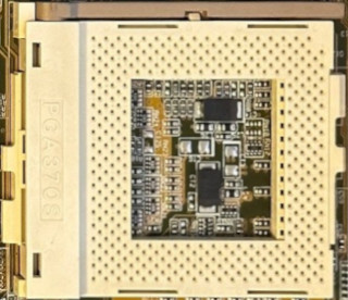
Socket 370S
Socket
The Intel Celeron 667 was a desktop processor with 1 core, that was never released. It is part of the Celeron lineup, using the Timna architecture with Socket 370S. Celeron 667 has 128 KB of L2 cache and operates at 667 MHz. Intel is making the Celeron 667 on a 180 nm production node, the transistor count is unknown. The multiplier is locked on Celeron 667, which limits its overclocking potential.
With a TDP of 30 W, the Celeron 667 consumes only little energy. The highest officially supported memory speed is 400 MT/s, but with overclocking (and the right memory modules) you can go even higher. Actual memory technology support depends on the chosen motherboard, the processor itself supports multiple memory types, but most motherboards have only one kind of slot. For communication with other components in the computer, Celeron 667 uses a PCI-Express N/A connection. This processor features the Intel i752 integrated graphics solution.
Many games will refuse to start on this processor due to the lack of the SSE2/SSE3/SSE4 instruction set.
Physical
| Socket: | Intel Socket 370S |
|---|---|
| Foundry: | Intel |
| Process Size: | 180 nm |
| Die Size: | 129 mm² |
| Package: | FC-PGA |
Processor
| Market: | Desktop |
|---|---|
| Production Status: | End-of-life |
| Release Date: | Never Released |
| Part#: | QV18 |
| Bundled Cooler: | None |
Performance
| Frequency: | 667 MHz |
|---|---|
| Turbo Clock: | N/A |
| Base Clock: | 133 MHz |
| Multiplier: | 5.0x |
| Multiplier Unlocked: | No |
| Voltage: | 1.65 V |
| TDP: | 30 W |
Architecture
| Codename: | Timna |
|---|---|
| Generation: |
Celeron
(Timna) |
| Memory Support: |
unknown
Depends on motherboard |
| Rated Speed: | 400 MT/s |
| Memory Bus: | Single-channel |
| ECC Memory: | No |
| PCI-Express: | N/A |
Core Config
| # of Cores: | 1 |
|---|---|
| # of Threads: | 1 |
| SMP # CPUs: | 1 |
| Integrated Graphics: | Intel i752 |
Cache
| Cache L1: | 32 KB |
|---|---|
| Cache L2: | 128 KB |
Features
|
Notes
| "Timna" was cancelled in 2000 but engineering samples were produced and distributed in small quantities along with sample platforms featuring both RDRAM and SDRAM variants. The processor die featured a sophisticated integration of a RDRAM memory controller and i752 graphics core as a means to decrease board complexity and cost. SDRAM boards were possible with the use of the Intel MTH translator chip which incurred a large performance penalty but further decreased cost at the time. |
Jul 5th, 2025 12:45 CDT
change timezone
Latest GPU Drivers
New Forum Posts
- FINAL FANTASY XIV: Dawntrail Official Benchmark (193)
- Are there others on TPU with a dual system (two pc´s in one case)? (9)
- How do you view TPU & the internet in general? (With poll) (69)
- TPU's Rosetta Milestones and Daily Pie Thread (2374)
- Have you got pie today? (16775)
- WCG Daily Numbers (12927)
- What are you playing? (23891)
- Folding Pie and Milestones!! (9606)
- TPU's Nostalgic Hardware Club (20483)
- [GPU-Z Test Build] New Kernel Driver, Everyone: Please Test (68)
Popular Reviews
- NVIDIA GeForce RTX 5050 8 GB Review
- Fractal Design Scape Review - Debut Done Right
- Crucial T710 2 TB Review - Record-Breaking Gen 5
- ASUS ROG Crosshair X870E Extreme Review
- PowerColor ALPHYN AM10 Review
- Sapphire Radeon RX 9060 XT Pulse OC 16 GB Review - An Excellent Choice
- Upcoming Hardware Launches 2025 (Updated May 2025)
- AMD Ryzen 7 9800X3D Review - The Best Gaming Processor
- Sapphire Radeon RX 9070 XT Nitro+ Review - Beating NVIDIA
- NVIDIA GeForce RTX 5060 8 GB Review
TPU on YouTube
Controversial News Posts
- Intel's Core Ultra 7 265K and 265KF CPUs Dip Below $250 (288)
- NVIDIA Grabs Market Share, AMD Loses Ground, and Intel Disappears in Latest dGPU Update (212)
- Some Intel Nova Lake CPUs Rumored to Challenge AMD's 3D V-Cache in Desktop Gaming (140)
- NVIDIA GeForce RTX 5080 SUPER Could Feature 24 GB Memory, Increased Power Limits (115)
- NVIDIA Launches GeForce RTX 5050 for Desktops and Laptops, Starts at $249 (105)
- Microsoft Partners with AMD for Next-gen Xbox Hardware (105)
- AMD Radeon RX 9070 XT Gains 9% Performance at 1440p with Latest Driver, Beats RTX 5070 Ti (102)
- Intel "Nova Lake‑S" Series: Seven SKUs, Up to 52 Cores and 150 W TDP (100)


