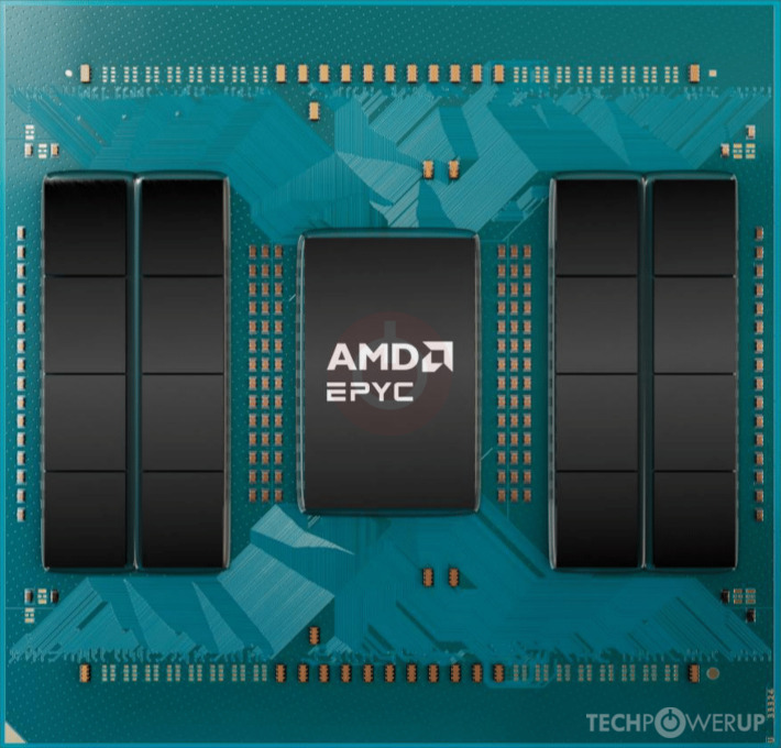
 / EPYC")
128
Cores
256
Threads
500 W
TDP
2.7 GHz
Frequency
4.1 GHz
Boost
Turin
Codename
Socket SP5
Socket

Front
Delidded

Die Shot

Back

Connectivity
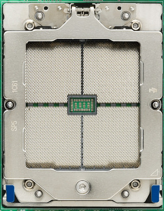
AMD Socket SP5
The AMD EPYC 9755 is a server/workstation processor with 128 cores, launched in October 2024, at an MSRP of $12984. It is part of the EPYC lineup, using the Zen 5 (Turin) architecture with Socket SP5. Thanks to AMD Simultaneous Multithreading (SMT) the core-count is effectively doubled, to 256 threads. To further increase overall system performance, up to two EPYC 9755 CPUs can link up in a multi-processor (SMP) configuration. EPYC 9755 has 512 MB of L3 cache and operates at 2.7 GHz by default, but can boost up to 4.1 GHz, depending on the workload. AMD is building the EPYC 9755 on a 4 nm production process using 133,040 million transistors. The silicon die of the chip is not fabricated at AMD, but at the foundry of TSMC. The multiplier is locked on EPYC 9755, which limits its overclocking capabilities.
With a TDP of 500 W, the EPYC 9755 is extremely power hungry, which means you need top-notch cooling. AMD's processor supports DDR5 memory with a twelve-channel interface. The highest officially supported memory speed is 6000 MT/s, but with overclocking (and the right memory modules) you can go even higher. ECC memory is supported, too, which is an important capability for mission-critical systems, to avoid data corruption. For communication with other components in the machine, EPYC 9755 uses a PCI-Express Gen 5 connection. This processor lacks integrated graphics, you might need a graphics card.
Hardware virtualization is available on the EPYC 9755, which greatly improves virtual machine performance. Programs using Advanced Vector Extensions (AVX) will run on this processor, boosting performance for calculation-heavy applications. Besides AVX, AMD has added support for the newer AVX2 and AVX-512 instructions, too.
Physical
| Socket: | AMD Socket SP5 |
|---|---|
| Foundry: | TSMC |
| Process Size: | 4 nm |
| Transistors: | 133,040 million |
| Die Size: | 16x 70.6 mm² |
| I/O Process Size: | 6 nm |
| Package: | FC-LGA6096 |
Processor
| Market: | Server/Workstation |
|---|---|
| Production Status: | Active |
| Release Date: | Oct 10th, 2024 |
| Launch Price: | $12984 |
| Part#: | 100-000001443 |
Performance
| Frequency: | 2.7 GHz |
|---|---|
| Turbo Clock: | up to 4.1 GHz |
| Base Clock: | 100 MHz |
| Multiplier: | 27.0x |
| Multiplier Unlocked: | No |
| TDP: | 500 W |
| Configurable TDP: | 450-500 W |
Architecture
| Codename: | Turin |
|---|---|
| Generation: |
EPYC
(Zen 5 (Turin)) |
| Memory Support: | DDR5 |
| Rated Speed: | 6000 MT/s |
| 2DPC Rated Speed: | 4400 MT/s |
| Memory Bus: | Twelve-channel |
| ECC Memory: | Yes |
| PCI-Express: |
Gen 5, 128 Lanes (CPU only) |
| CXL: | Gen 2.0 |
Core Config
| # of Cores: | 128 |
|---|---|
| # of Threads: | 256 |
| SMP # CPUs: | 2 |
| Integrated Graphics: | N/A |
Cache
| Cache L1: | 80 KB (per core) |
|---|---|
| Cache L2: | 1 MB (per core) |
| Cache L3: | 512 MB (shared) |
Features
|
Notes
| CXL 2.0 supports Type 3 devices which can provide significant increases to system attached DRAM capacity. SEV-SNP security features extend to Type 3 devices. AMD's "Turin" CPUs can be configured for DDR5 6400 MT/s with 1 DIMM per channel (1DPC) in specific scenarios, but 6000 MT/s is the official supported rating for the SP5 platform with firmware updates provided. |
Oct 15th, 2024 11:17 EDT
change timezone
Latest GPU Drivers
New Forum Posts
- No AMD ITX mobo for you? (25)
- Intel N100 based micro ATX boards (31)
- Looking for a a new low power trio for my home studio (4)
- Apparently nuclear power is easy to do. 2030 it goes online, just announced today... talk about fast. (1)
- so whats with evga? (142)
- Are Firecuda 530 TBW ratings legit? (3)
- [newegg] B550 Motherboard and Ryzen 7 5700x combo for $279.99 (9)
- Which 20 TB drive to get? (98)
- Any way to prevent screen from "Blacking Out" when resizing/rescaling? (5)
- Large discrepancy in Win98 graphics performance of X850 XT PE (15)
Popular Reviews
- Intel Core Ultra Arrow Lake Preview
- Silent Hill 2 Remake Performance Benchmark Review - 35 GPUs Tested
- Lian Li O11 Vision Compact Review
- Silent Hill 2 Remake Handheld Performance Review
- Silent Hill 2 Remake: DLSS vs. FSR vs. XeSS Comparison Review
- Klevv CRAS C925 2 TB Review
- Upcoming Hardware Launches 2024 (Updated Jul 2024)
- Montech King 65 Pro Review
- AMD Ryzen 9 9950X Review - The New Flagship
- AMD Ryzen 7 9700X Review - The Magic of Zen 5
Controversial News Posts
- NVIDIA GeForce RTX 5090 and RTX 5080 Specifications Surface, Showing Larger SKU Segmentation (183)
- AMD Ryzen 9 9950X3D and 9900X3D to Feature 3D V-cache on Both CCD Chiplets (127)
- MSI OCLab Reveals Ryzen 9000X3D 11-13% Faster Than 7000X3D, AMD Set to Dominate "Arrow Lake" in Gaming (123)
- Quick Denuvo DRM Cracks Cost Game Publishers 20% in Revenue, According to Study (117)
- AMD Rushing in Ryzen 7 9800X3D, Expect Product Launch Late-October (117)
- Single-Player Games Lose to PVP in Younger Audiences Despite Recent Hits (116)
- NVIDIA Tunes GeForce RTX 5080 GDDR7 Memory to 32 Gbps, RTX 5070 Launches at CES (112)
- Intel's Core Ultra 9 285K Performance Claims Leaked, Doesn't Beat i9-14900K at Gaming (111)