8
Cores
16
Threads
45 W
TDP
3.8 GHz
Frequency
5.1 GHz
Boost
Hawk Point
Codename
Socket FP8
Socket
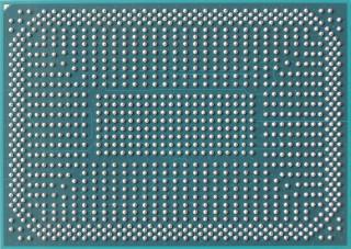
The AMD Ryzen 7 260 is a mobile processor with 8 cores, launched in January 2025. It is part of the Ryzen 7 lineup, using the Zen 4 (Hawk Point) architecture with Socket FP8. Thanks to AMD Simultaneous Multithreading (SMT) the core-count is effectively doubled, to 16 threads. Ryzen 7 260 has 16 MB of L3 cache and operates at 3.8 GHz by default, but can boost up to 5.1 GHz, depending on the workload. AMD is making the Ryzen 7 260 on a 4 nm production node using 25,000 million transistors. The silicon die of the chip is not fabricated at AMD, but at the foundry of TSMC. The multiplier is locked on Ryzen 7 260, which limits its overclocking potential.
With a TDP of 45 W, the Ryzen 7 260 consumes typical power levels for a modern PC. AMD's processor supports DDR5 memory with a dual-channel interface. The highest officially supported memory speed is 5600 MT/s, but with overclocking (and the right memory modules) you can go even higher. For communication with other components in the machine, Ryzen 7 260 uses a PCI-Express Gen 4 connection. This processor features the Radeon 780M integrated graphics solution.
Hardware virtualization is available on the Ryzen 7 260, which greatly improves virtual machine performance. Programs using Advanced Vector Extensions (AVX) can run on this processor, boosting performance for calculation-heavy applications. Besides AVX, AMD has added support for the newer AVX2 and AVX-512 instructions, too.
Physical
| Socket: | AMD Socket FP8 |
|---|---|
| Foundry: | TSMC |
| Process Size: | 4 nm |
| Transistors: | 25,000 million |
| Die Size: | 178 mm² |
| Package: | FP8, FP7, FP7r2 |
| tJMax: | 100°C |
Processor
| Market: | Mobile |
|---|---|
| Production Status: | Active |
| Release Date: | Jan 6th, 2025 |
| Part#: | 100-000001724 |
Performance
| Frequency: | 3.8 GHz |
|---|---|
| Turbo Clock: | up to 5.1 GHz |
| Base Clock: | 100 MHz |
| Multiplier: | 38.0x |
| Multiplier Unlocked: | No |
| XDNA NPU: | 16 TOPS |
| TDP: | 45 W |
| Configurable TDP: | 35-54 W |
Architecture
| Codename: | Hawk Point |
|---|---|
| Generation: |
Ryzen 7
(Zen 4 (Hawk Point)) |
| Memory Support: | DDR5 |
| LPDDR5x Speed: | 7500 MT/s |
| Rated Speed: | 5600 MT/s |
| Memory Bus: | Dual-channel |
| ECC Memory: | No |
| PCI-Express: |
Gen 4, 20 Lanes (CPU only) |
Core Config
| # of Cores: | 8 |
|---|---|
| # of Threads: | 16 |
| SMP # CPUs: | 1 |
| Integrated Graphics: | Radeon 780M |
Cache
| Cache L1: | 64 KB (per core) |
|---|---|
| Cache L2: | 1 MB (per core) |
| Cache L3: | 16 MB (shared) |
Features
|
Notes
| Graphics engine boost clock: 2700MHz Int8 TOPS rated at up to 38 TOPS combining CPU cores, GPU cores, and NPU. |
Jan 17th, 2025 14:40 EST
change timezone
Latest GPU Drivers
New Forum Posts
- GTX 1650 bottlenecks 6th gen i5 (7)
- Polychrome changing screen resolution on startup (0)
- Motherboard ground connector not picking on mulitimeter (9)
- Sapphire pulse rx 7900 gre memory overclock (28)
- TPU's F@H Team (20389)
- Limit Reasons issues (3)
- New GameTech GPU benchmark. Share your results! (STEAM page live now) (224)
- What DLSS/FSR Upscaling Mode do you use? (119)
- Blackwell GPU die sizes revealed; regression in some cases (24)
- What are you playing? (22605)
Popular Reviews
- NVIDIA GeForce RTX 50 Technical Deep Dive
- ASRock Arc B570 Challenger OC Review
- ASUS ROG Strix B860-A Gaming Wi-Fi Review
- AMD Ryzen 7 9800X3D Review - The Best Gaming Processor
- G-Wolves Hati-S2 8K Review
- Fosi Audio K7 Gaming Desktop DAC/Headphone Amplifier Review
- Sparkle B570 Guardian OC Review
- ThieAudio Origin In-Ear Monitors Review - Basshead Love
- GPU Test System Update for 2025
- Quick Look: Huion Kamvas 16 (Gen 3) Graphics Tablet
Controversial News Posts
- NVIDIA 2025 International CES Keynote: Liveblog (468)
- AMD Debuts Radeon RX 9070 XT and RX 9070 Powered by RDNA 4, and FSR 4 (348)
- NVIDIA GeForce RTX 5090 Features 575 W TDP, RTX 5080 Carries 360 W TDP (217)
- AMD Radeon RX 9070 XT Alleged Benchmark Leaks, Underwhelming Performance (204)
- AMD Radeon RX 9070 XT & RX 9070 Custom Models In Stock at European Stores (189)
- Potential RTX 5090 and RTX 5080 Pricing in China Leaks (173)
- AMD Radeon RX 9070 XT Tested in Cyberpunk 2077 and Black Myth: Wukong (168)
- AMD Radeon RX 9070 XT Boosts up to 3.10 GHz, Board Power Can Reach up to 330W (167)


