8
Cores
16
Threads
28 W
TDP
2000 MHz
Frequency
5 GHz
Boost
Krackan Point
Codename
Socket FP8
Socket
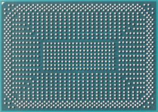
The AMD Ryzen AI 7 350 is a mobile processor with 8 cores, launched in January 2025. It is part of the Ryzen AI lineup, using the Zen 5 architecture with Socket FP8. Thanks to AMD Simultaneous Multithreading (SMT) the core-count is effectively doubled, to 16 threads. Ryzen AI 7 350 has 8 MB of L3 cache and operates at 2000 MHz by default, but can boost up to 5 GHz, depending on the workload. AMD is making the Ryzen AI 7 350 on a 4 nm production node, the transistor count is unknown. The silicon die of the chip is not fabricated at AMD, but at the foundry of TSMC. The multiplier is locked on Ryzen AI 7 350, which limits its overclocking potential.
With a TDP of 28 W, the Ryzen AI 7 350 consumes only little energy. AMD's processor supports DDR5 memory with a dual-channel interface. The highest officially supported memory speed is 5600 MT/s, but with overclocking (and the right memory modules) you can go even higher. For communication with other components in the machine, Ryzen AI 7 350 uses a PCI-Express Gen 4 connection. This processor features the Radeon 860M integrated graphics solution.
Hardware virtualization is available on the Ryzen AI 7 350, which greatly improves virtual machine performance. Programs using Advanced Vector Extensions (AVX) can run on this processor, boosting performance for calculation-heavy applications. Besides AVX, AMD has added support for the newer AVX2 and AVX-512 instructions, too.
Physical
| Socket: | AMD Socket FP8 |
|---|---|
| Foundry: | TSMC |
| Process Size: | 4 nm |
| Package: | FP8 |
| tJMax: | 100°C |
Processor
| Market: | Mobile |
|---|---|
| Production Status: | Active |
| Release Date: | Jan 6th, 2025 |
| Part#: | 100-000001601 |
Performance
| Frequency: | 2000 MHz |
|---|---|
| Turbo Clock: | up to 5 GHz |
| E-Core Frequency: |
2000 MHz
up to 3.5 GHz |
| Base Clock: | 100 MHz |
| Multiplier: | 20.0x |
| Multiplier Unlocked: | No |
| XDNA NPU: | 50 TOPS |
| TDP: | 28 W |
| Configurable TDP: | 15-54 W |
Architecture
| Codename: | Krackan Point |
|---|---|
| Generation: |
Ryzen AI
(Zen 5) |
| Memory Support: | DDR5 |
| LPDDR5x Speed: | 8000 MT/s |
| Rated Speed: | 5600 MT/s |
| Memory Bus: | Dual-channel |
| ECC Memory: | No |
| PCI-Express: |
Gen 4, 16 Lanes (CPU only) |
Core Config
| # of Cores: | 8 |
|---|---|
| # of Threads: | 16 |
| Hybrid Cores: | 4 + 4 |
| SMP # CPUs: | 1 |
| Integrated Graphics: | Radeon 860M |
Cache
| Cache L1: | 80 KB (per core) |
|---|---|
| Cache L2: | 1 MB (per core) |
| Cache L3: | 8 MB |
| E-Core L3: | 8 MB |
Features
|
Notes
| Radeon Graphics dynamic frequency: 400-3000 MHz |
Jan 15th, 2025 04:17 EST
change timezone
Latest GPU Drivers
New Forum Posts
- RTX 5090 will have liquid metal on founder's edition, but will the 5080, 5070 ti FE's? (16)
- How many are using 24h2? Problems still? (202)
- The TPU UK Clubhouse (25628)
- Hello, I bought a RAM from Shadow RGB DDR5-4800 on a b650 amd board, but it does not work. NTSRD5P48DP-16s (29)
- Need to set expectations... (4)
- AGESA PI 1.2.0.3 benchmarked. (0)
- Microsoft Officially drops AC3 (Dolby Digital) Support from W11 24H2 (12)
- 9800x 3d vs 12900k - Battle of the Century (439)
- i7-7700k upgrade to 5700X3D worth it? (138)
- Advice please - AMD Radeon RX 5700 XT - PC Restarts (45)
Popular Reviews
- AMD Ryzen 7 9800X3D Review - The Best Gaming Processor
- ASUS ROG Strix B860-A Gaming Wi-Fi Review
- ThieAudio Origin In-Ear Monitors Review - Basshead Love
- LAMZU Maya X Review
- ASUS ROG Strix B850-F Gaming WiFi Review
- GPU Test System Update for 2025
- Upcoming Hardware Launches 2024 (Updated Nov 2024)
- Arrow Lake Retested with Latest 24H2 Updates and 0x114 Microcode
- Royal Kludge S85 TKL Wireless Mechanical Keyboard Review
- HEDDphone TWO GT Air Motion Transformer Headphones Review
Controversial News Posts
- NVIDIA 2025 International CES Keynote: Liveblog (467)
- AMD Debuts Radeon RX 9070 XT and RX 9070 Powered by RDNA 4, and FSR 4 (348)
- NVIDIA GeForce RTX 5090 Features 575 W TDP, RTX 5080 Carries 360 W TDP (212)
- AMD Radeon RX 9070 XT Alleged Benchmark Leaks, Underwhelming Performance (204)
- 32 GB NVIDIA RTX 5090 To Lead the Charge As 5060 Ti Gets 16 GB Upgrade and 5060 Still Stuck With Last-Gen VRAM Spec (174)
- Potential RTX 5090 and RTX 5080 Pricing in China Leaks (173)
- AMD Radeon RX 9070 XT Boosts up to 3.10 GHz, Board Power Can Reach up to 330W (167)
- AMD Radeon RX 9070 XT Tested in Cyberpunk 2077 and Black Myth: Wukong (164)


