Report an Error


NVIDIA C73
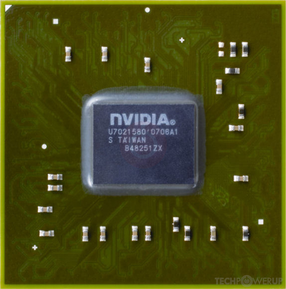
C73

NF-7050-630i-A1
NVIDIA's C73 GPU uses the Curie architecture and is made using a 90 nm production process. With a die size of 81 mm² and a transistor count of 112 million it is a very small chip. C73 supports DirectX 9.0c (Feature Level 9_3). For GPU compute applications, OpenCL version N/A can be used. It features 4 pixel shaders and 1 vertex shaders, 2 texture mapping units and 2 ROPs. Due to the lack of unified shaders you will not be able to run recent games at all (which require unified shader/DX10+ support).
Graphics Processor
- Released
- Oct 4th, 2007
- GPU Name
- C73
- Codename
- NV73
- Architecture
- Curie
- Process Size
- 90 nm
- Transistors
- 112 million
- Density
- 1.4M / mm²
- Die Size
- 81 mm²
Graphics Features
- DirectX
- 9.0c (9_3)
- OpenGL
-
2.0 (full)
2.1 (partial)
- OpenCL
- N/A
- Vulkan
- N/A
- Shader Model
- 3.0
- WDDM
- 1.0
- PureVideo HD
- VP1
- VDPAU
- No Support
Render Config
- Pixel Shaders
- 4
- Vertex Shaders
- 1
- TMUs
- 2
- ROPs
- 2
All Curie GPUs
NVIDIA GPU Architecture History
- 2025 Blackwell 2.0
- 2024 Blackwell
- 2023 Hopper
- 2022-2024 Ada Lovelace
- 2020-2024 Ampere
- 2018-2022 Turing
- 2017-2020 Volta
- 2016-2021 Pascal
- 2014-2019 Maxwell 2.0
- 2014-2017 Maxwell
- 2013-2015 Kepler 2.0
- 2012-2018 Kepler
- 2010-2016 Fermi 2.0
- 2010-2013 VLIW Vec4
- 2010-2016 Fermi
- 2007-2013 Tesla 2.0
- 2006-2010 Tesla
- 2003-2013 Curie
- 2003-2005 Rankine
- 2001-2003 Kelvin
- 1999-2005 Celsius
- 1998-2000 Fahrenheit
Graphics cards using the NVIDIA C73 GPU
| Name | Chip | Memory | Shaders | TMUs | ROPs | Base Clock | Boost Clock | Memory Clock |
|---|---|---|---|---|---|---|---|---|
| NF-7050-630i-A1 | System Shared | 2 / 1 | 2 | 2 | 500 MHz | 630 MHz | System Shared | |
| NF-7150-610i-A1 | System Shared | 2 / 1 | 2 | 2 | 630 MHz | System Shared | ||
| NF-7100 | System Shared | 4 / 1 | 2 | 2 | 600 MHz | System Shared | ||
| NF-7050-620i-A1 | System Shared | 2 / 1 | 2 | 2 | 500 MHz | 630 MHz | System Shared |


C73 GPU Notes
| PureVideo HD: VP1 VDPAU: No Support |
Jul 3rd, 2024 21:05 EDT
change timezone
Latest GPU Drivers
New Forum Posts
- Asrock 5700XT Phantom Gaming D has the wrong Vbios (14)
- The TPU UK Clubhouse (24927)
- Intel Core "Special Edition" Owners' Club (75)
- Does TPU use Google-Tracking? (56)
- New GameTech GPU benchmark. Share your results! (11)
- Samsung 990 Pro (2TB) - Very poor random read and write performance (9)
- What is the PC monitors future trend in terms of resolution and aspect ratio? (54)
- Bykski Memory Heat Spreader -DDR5/TridentZ5 (10)
- Can someone help me with getting my ram stable? (4)
- ELSA RADEON RX 580 8GB GDDR5 256BIT (3)
Popular Reviews
- Gigabyte GS34WQC Review - An Affordable Ultrawide
- AMD FidelityFX FSR 3.1 Review - Frame Generation for Everyone
- The First Descendant Performance Benchmark Review - 30 GPUs Tested
- Lian Li HydroShift LCD 360S AIO Review
- Upcoming Hardware Launches 2024 (Updated May 2024)
- Endgame Gear OP1 8K Review
- AMD Ryzen 7 7800X3D Review - The Best Gaming CPU
- XFX Radeon RX 7900 XTX Magnetic Air Review
- Corsair MP600 Mini 2 TB Review - Great Storage for Steam Deck
- Thermalright Phantom Spirit 120 EVO Review
Controversial News Posts
- Legendary Overclocker KINGPIN Leaves EVGA and Joins PNY to Develop Next-Generation GPUs for Extreme OC (195)
- AMD Says Ryzen 9000 Series Won't Beat 7000X3D Series at Gaming (141)
- Possible Specs of NVIDIA GeForce "Blackwell" GPU Lineup Leaked (140)
- Noctua Announces $150 Flagship NH-D15 G2 CPU Coolers and NF-A14x25r G2 140mm Fans (131)
- First Reviews are Live and Snapdragon X Elite Doesn't Quite Deliver on Promised Performance (124)
- Microsoft Closer to Removing Local Accounts from Windows 11, Removes Help Page on How to Switch to One (121)
- ASUS Enhances Customer Support Following Gamers Nexus Investigation (118)
- Nightmare Fuel for Intel: Arm CEO Predicts Arm will Take Over 50% Windows PC Market-share by 2029 (112)