Report an Error


NVIDIA Quadro FX 3700
- Graphics Processor
- G92
- Cores
- 112
- TMUs
- 56
- ROPs
- 16
- Memory Size
- 512 MB
- Memory Type
- GDDR3
- Bus Width
- 256 bit

GPU
I/O

Bottom

Back
Recommended Gaming Resolutions:
- 1280x720
- 1366x768
- 1600x900
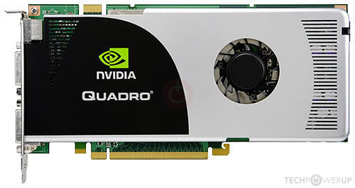
The Quadro FX 3700 was an enthusiast-class professional graphics card by NVIDIA, launched on January 8th, 2008. Built on the 65 nm process, and based on the G92 graphics processor, in its G92-875-A2 variant, the card supports DirectX 11.1. Even though it supports DirectX 11, the feature level is only 10_0, which can be problematic with many DirectX 11 & DirectX 12 titles. The G92 graphics processor is a large chip with a die area of 324 mm² and 754 million transistors. Unlike the fully unlocked GeForce 8800 GTS 512, which uses the same GPU but has all 128 shaders enabled, NVIDIA has disabled some shading units on the Quadro FX 3700 to reach the product's target shader count. It features 112 shading units, 56 texture mapping units, and 16 ROPs. NVIDIA has paired 512 MB GDDR3 memory with the Quadro FX 3700, which are connected using a 256-bit memory interface. The GPU is operating at a frequency of 500 MHz, memory is running at 800 MHz.
Being a single-slot card, the NVIDIA Quadro FX 3700 draws power from 1x 6-pin power connector, with power draw rated at 78 W maximum. Display outputs include: 2x DVI, 1x S-Video. Quadro FX 3700 is connected to the rest of the system using a PCI-Express 2.0 x16 interface. The card measures 267 mm in length, 111 mm in width, and features a single-slot cooling solution. Its price at launch was 1599 US Dollars.
Being a single-slot card, the NVIDIA Quadro FX 3700 draws power from 1x 6-pin power connector, with power draw rated at 78 W maximum. Display outputs include: 2x DVI, 1x S-Video. Quadro FX 3700 is connected to the rest of the system using a PCI-Express 2.0 x16 interface. The card measures 267 mm in length, 111 mm in width, and features a single-slot cooling solution. Its price at launch was 1599 US Dollars.
Graphics Processor
Graphics Card
- Release Date
- Jan 8th, 2008
- Generation
-
Quadro FX Tesla
(x700)
- Predecessor
- Quadro FX Curie
- Successor
- Quadro Fermi
- Production
- End-of-life
- Launch Price
- 1,599 USD
- Bus Interface
- PCIe 2.0 x16
- Reviews
- 26 in our database
Relative Performance
Based on TPU review data: "Performance Summary" at 1920x1080, 4K for 2080 Ti and faster.
Performance estimated based on architecture, shader count and clocks.
Clock Speeds
- GPU Clock
- 500 MHz
- Shader Clock
- 1250 MHz
- Memory Clock
-
800 MHz
1600 Mbps effective
Memory
- Memory Size
- 512 MB
- Memory Type
- GDDR3
- Memory Bus
- 256 bit
- Bandwidth
- 51.20 GB/s
Render Config
- Shading Units
- 112
- TMUs
- 56
- ROPs
- 16
- SM Count
- 14
- L2 Cache
- 64 KB
Theoretical Performance
- Pixel Rate
- 8.000 GPixel/s
- Texture Rate
- 28.00 GTexel/s
- FP32 (float)
- 280.0 GFLOPS
Board Design
- Slot Width
- Single-slot
- Length
- 267 mm
10.5 inches
- Width
- 111 mm
4.4 inches
- TDP
- 78 W
- Suggested PSU
- 250 W
- Outputs
- 2x DVI
1x S-Video
- Power Connectors
- 1x 6-pin
- Board Number
- Q393 SKU 503
Graphics Features
- DirectX
- 11.1 (10_0)
- OpenGL
- 3.3
- OpenCL
- 1.1
- Vulkan
- N/A
- CUDA
- 1.1
- Shader Model
- 4.0
G92 GPU Notes
| PureVideo HD: VP2 VDPAU: Feature Set A Latest Drivers: Windows 2000: Quadro Release 261.19 Windows XP / Server 2003 x64: GeForce Release 185.81 (Notebooks) GeForce Release 340.52 Quadro Release R319 U2 (321.01) Tesla Release 258.96 Windows Vista: GeForce Release 307.83 (Notebooks) GeForce Release 342.01 Quadro Release R340 U15 (342.01) Tesla Release 258.96 Windows 7 / 8 / 8.1 / 10: GeForce Release 342.01 Quadro Release R340 U15 (342.01) Tesla Release 258.96 |
Apr 13th, 2025 21:33 EDT
change timezone
Latest GPU Drivers
New Forum Posts
- Lian Li O11 Dynamic XL ROG. (14)
- Regarding fan noise (16)
- Why PC Gaming rocks (13)
- What local LLM-s you use? (159)
- GCN less stable on AM4 than 2011-3? (6)
- Rare GPUs / Unreleased GPUs (2068)
- SK hynix A-Die (Overclocking thread) only for RYZEN AM5 users (31)
- RX 9000 series GPU Owners Club (311)
- Upgrade for a GTX-1060 video card to a X570 AM4 MB w/ a Ryzen 9 3900X (19)
- Gigabyte 5090 Aorus Master VRM Specs (21)
Popular Reviews
- TerraMaster F8 SSD Plus Review - Compact and quiet
- ASUS GeForce RTX 5080 TUF OC Review
- Thermaltake TR100 Review
- The Last Of Us Part 2 Performance Benchmark Review - 30 GPUs Compared
- Zotac GeForce RTX 5070 Ti Amp Extreme Review
- Sapphire Radeon RX 9070 XT Pulse Review
- Sapphire Radeon RX 9070 XT Nitro+ Review - Beating NVIDIA
- Upcoming Hardware Launches 2025 (Updated Apr 2025)
- MSI MAG CORELIQUID A15 360 Review
- ASRock Z890 Taichi OCF Review
Controversial News Posts
- NVIDIA GeForce RTX 5060 Ti 16 GB SKU Likely Launching at $499, According to Supply Chain Leak (181)
- MSI Doesn't Plan Radeon RX 9000 Series GPUs, Skips AMD RDNA 4 Generation Entirely (146)
- Microsoft Introduces Copilot for Gaming (124)
- NVIDIA Sends MSRP Numbers to Partners: GeForce RTX 5060 Ti 8 GB at $379, RTX 5060 Ti 16 GB at $429 (124)
- Nintendo Confirms That Switch 2 Joy-Cons Will Not Utilize Hall Effect Stick Technology (105)
- Over 200,000 Sold Radeon RX 9070 and RX 9070 XT GPUs? AMD Says No Number was Given (100)
- Nintendo Switch 2 Launches June 5 at $449.99 with New Hardware and Games (99)
- NVIDIA PhysX and Flow Made Fully Open-Source (77)