Report an Error
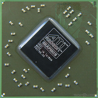
ATI FirePro V7750
- Graphics Processor
- RV730
- Cores
- 320
- TMUs
- 32
- ROPs
- 8
- Memory Size
- 1024 MB
- Memory Type
- GDDR3
- Bus Width
- 128 bit
Recommended Gaming Resolutions:
- 1366x768
- 1600x900
- 1920x1080
The FirePro V7750 was an enthusiast-class professional graphics card by ATI, launched on March 27th, 2009. Built on the 55 nm process, and based on the RV730 graphics processor, in its RV730 GL V7750 variant, the card supports DirectX 10.1. Since FirePro V7750 does not support DirectX 11 or DirectX 12, it might not be able to run all the latest games. The RV730 graphics processor is an average sized chip with a die area of 146 mm² and 514 million transistors. It features 320 shading units, 32 texture mapping units, and 8 ROPs. ATI has paired 1,024 MB GDDR3 memory with the FirePro V7750, which are connected using a 128-bit memory interface. The GPU is operating at a frequency of 800 MHz, memory is running at 900 MHz.
Being a single-slot card, the ATI FirePro V7750 draws power from 1x 6-pin power connector, with power draw rated at 76 W maximum. Display outputs include: 1x DVI, 2x DisplayPort 1.0. FirePro V7750 is connected to the rest of the system using a PCI-Express 2.0 x16 interface. The card measures 234 mm in length, 111 mm in width, and features a single-slot cooling solution. Its price at launch was 799 US Dollars.
Being a single-slot card, the ATI FirePro V7750 draws power from 1x 6-pin power connector, with power draw rated at 76 W maximum. Display outputs include: 1x DVI, 2x DisplayPort 1.0. FirePro V7750 is connected to the rest of the system using a PCI-Express 2.0 x16 interface. The card measures 234 mm in length, 111 mm in width, and features a single-slot cooling solution. Its price at launch was 799 US Dollars.
Graphics Processor
Graphics Card
- Release Date
- Mar 27th, 2009
- Generation
-
FirePro Terascale
(Vx700)
- Predecessor
- FireGL
- Successor
- Radeon Pro GCN
- Production
- End-of-life
- Launch Price
- 799 USD
- Bus Interface
- PCIe 2.0 x16
- Reviews
- 10 in our database
Relative Performance
Based on TPU review data: "Performance Summary" at 1920x1080, 4K for 2080 Ti and faster.
Performance estimated based on architecture, shader count and clocks.
Clock Speeds
- GPU Clock
- 800 MHz
- Memory Clock
-
900 MHz
1800 Mbps effective
Memory
- Memory Size
- 1024 MB
- Memory Type
- GDDR3
- Memory Bus
- 128 bit
- Bandwidth
- 28.80 GB/s
Render Config
- Shading Units
- 320
- TMUs
- 32
- ROPs
- 8
- Compute Units
- 4
- L1 Cache
- 16 KB (per CU)
- L2 Cache
- 128 KB
Theoretical Performance
- Pixel Rate
- 6.400 GPixel/s
- Texture Rate
- 25.60 GTexel/s
- FP32 (float)
- 512.0 GFLOPS
Board Design
- Slot Width
- Single-slot
- Length
- 234 mm
9.2 inches
- Width
- 111 mm
4.4 inches
- TDP
- 76 W
- Suggested PSU
- 250 W
- Outputs
- 1x DVI
2x DisplayPort 1.0
- Power Connectors
- 1x 6-pin
- Board Number
- 109-B73061-00A
Graphics Features
- DirectX
- 10.1 (10_1)
- OpenGL
- 3.3
- OpenCL
- 1.1
- Vulkan
- N/A
- Shader Model
- 4.1
RV730 GPU Notes
| Mobile Variant: M96 Codename: Mario Graphics/Compute: GFX3 Display Core Engine: 3.2 Unified Video Decoder: 2.2 Latest Drivers: Windows XP / 8: Catalyst Software Suite 13.1 / 13.4 Beta Windows Vista / 7: Catalyst Software Suite 13.9 |
Retail boards based on this design (2)
| Name | GPU Clock | Memory Clock | Other Changes |
|---|---|---|---|
| 800 MHz | 900 MHz | ||
| 800 MHz | 900 MHz |
Apr 6th, 2025 13:56 EDT
change timezone
Latest GPU Drivers
New Forum Posts
- What local LLM-s you use? (146)
- How I made an Ultimate Cooling Guide (14)
- RX 9000 series GPU Owners Club (191)
- My computer setup - Request for opinions (29)
- Do you use Linux? (558)
- gpu heirarchy/performance/benchmarks- whos lying? (37)
- dropped my xbox controller, now LB doesn't feel clicky (9)
- I have a bricked XFX Radeon RX 580 8GB GPU. HELP! (11)
- Adventure: Running 8/9th gen Coffee Lake CPUs on Z170 motherboard (ASUS Maximus VIII Ranger) (377)
- Sapphire RX9070XT Nitro+ fan and high temperature problem (8)
Popular Reviews
- ASUS Prime X870-P Wi-Fi Review
- UPERFECT UStation Delta Max Review - Two Screens In One
- PowerColor Radeon RX 9070 Hellhound Review
- Corsair RM750x Shift 750 W Review
- DDR5 CUDIMM Explained & Benched - The New Memory Standard
- Upcoming Hardware Launches 2025 (Updated Apr 2025)
- Sapphire Radeon RX 9070 XT Pulse Review
- Sapphire Radeon RX 9070 XT Nitro+ Review - Beating NVIDIA
- AMD Ryzen 7 9800X3D Review - The Best Gaming Processor
- Pwnage Trinity CF Review
Controversial News Posts
- MSI Doesn't Plan Radeon RX 9000 Series GPUs, Skips AMD RDNA 4 Generation Entirely (146)
- Microsoft Introduces Copilot for Gaming (124)
- NVIDIA GeForce RTX 5060 Ti 16 GB SKU Likely Launching at $499, According to Supply Chain Leak (124)
- AMD Radeon RX 9070 XT Reportedly Outperforms RTX 5080 Through Undervolting (119)
- NVIDIA Reportedly Prepares GeForce RTX 5060 and RTX 5060 Ti Unveil Tomorrow (115)
- Over 200,000 Sold Radeon RX 9070 and RX 9070 XT GPUs? AMD Says No Number was Given (100)
- NVIDIA GeForce RTX 5050, RTX 5060, and RTX 5060 Ti Specifications Leak (97)
- Nintendo Switch 2 Launches June 5 at $449.99 with New Hardware and Games (92)


