Apr 16th, 2025 10:07 EDT change timezone

New Forum Posts

Popular Reviews

Controversial News Posts

News Posts matching #1 nm

Return to Keyword Browsing

Insider Report Suggests Start of 1 nm Chip Development at Samsung, Alleged 2029 Mass Production Phase Targeted

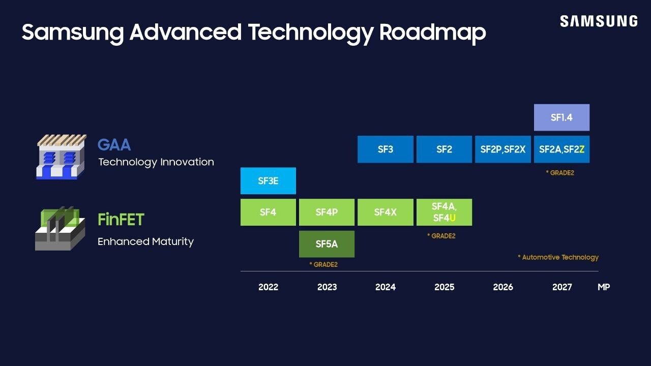
Samsung's foundry business seems to be busying itself with the rumored refinement of a 2 nm GAA (SF2) manufacturing node process—for possible mass production by the end of 2025, but company leadership will very likely be considering longer term goals. Mid-way through last month, industry moles posited that the megacorporation's semiconductor branch was questioning the future of a further out 1.4 nm (SF1.4) production line. Officially published roadmaps have this advanced technology rolling out by 2027. Despite present day "turmoil," insiders believe that a new team has been established—tasked with the creation of a so-called "dream semiconductor process." According to a fresh Sedaily news article, this fledgling department has started development of a 1 nm foundry process.

Anonymous sources claim that Samsung executives are keeping a watchful eye on a main competitor—as stated in the latest South Korean report: "there is a realistic gap with Taiwan's TSMC in technologies that are close to mass production, such as the 2 nm process, the company plans to speed up the development of the 1 nm process, a future technology, to create an opportunity for a turnaround." A portion of the alleged "1 nm development chip team" reportedly consists of veteran researchers from prior-gen projects. Semiconductor industry watchdogs theorize that a canceled SF1.4 line could be replaced by an even more advanced process. Sedaily outlined necessary hardware upgrades: "the 1.0 nanometer process requires a new technology concept that breaks the mold of existing designs as well as the introduction of next-generation equipment such as high-NA EUV exposure equipment. The company is targeting mass production after 2029." Samsung's current Advanced Technology Roadmap does not extend beyond 2027—inside sources claim that the decision to roll with 1.0 nm was made at some point last month.

DNP Achieves Fine Pattern Resolution on EUV Lithography Photomasks for Beyond 2nm Generation

Dai Nippon Printing Co., Ltd. (DNP) has successfully achieved the fine pattern resolution required for photomasks for logic semiconductors of the beyond 2 nm (nm: 10-9 meter) generation that support Extreme Ultra-Violet (EUV) lithography, a cutting-edge process in semiconductor manufacturing.

DNP has also completed the criteria evaluation for photomasks compatible with High-Numerical Aperture, the application being considered for next-generation semiconductors beyond the 2 nm generation, and has commenced the supply of evaluation photomasks. High-NA EUV lithography makes it possible to form fine patterns on silicon wafers with a higher resolution than previously possible, and is expected to lead to the realization of high-performance, low-power semiconductors.

South Korean Research Team Develops Method to Grow Sub-Nanometer Transistors

A research team from the South Korean Institute for Basic Science (IBS) has developed a new method for growing 1D metallic materials less than 1 nm wide. They applied this technique to create a new structure for 2D semiconductor logic circuits, using the 1D metals as gate electrodes in very small transistors. However, creating very small transistors that can control electron movement within a few nanometers has been challenging. The size of semiconductor devices depends on the width and efficiency of the gate electrode. Current manufacturing processes can't make gate lengths below a few nanometers due to limitations in lithography. To address this, the team used the mirror twin boundary (MTB) of molybdenum disulfide, which is a 1D metal only 0.4 nm wide, as a gate electrode. The IBS team achieved the 1D MTB metallic phase by altering the crystal structure of a 2D semiconductor at the atomic level.

The International Roadmap for Devices and Systems (IRDS) predicts semiconductor technology to reach about 0.5 nm by 2037, with transistor gate lengths of 12 nm. The research team's transistor demonstrated a channel width as small as 3.9 nm, surpassing this prediction. The 1D MTB-based transistor also offers advantages in circuit performance. Unlike some current technologies (FinFETs or GAA) that face issues with parasitic capacitance in highly integrated circuits, this new transistor can minimize such problems due to its simple structure and narrow gate width.

Intel 10A (1 nm-class) Node to Enter Mass Production in 2027

Last week at the Intel Foundry Services Connect event, Intel unveiled its Intel 14A foundry node (1.4 nm-class), to succeed its Intel 18A and Intel 20A nodes, with mass production on this node expected to commence in 2026. It turns out that there is an even more advanced node Intel is working on, which it didn't announce last week, but which was part of an NDA presentation that the company forgot to lift. We're talking about the new Intel 10A node, a 1 nm-class silicon fabrication node that's a generation ahead of Intel 20A. The company says that it expects mass production on the node to begin toward the end of 2027. It is on the backs of these sub-2 nm class nodes, and the impending organizational changes that sees Intel Foundry Services become a more independent commercial entity, that Intel CEO Pat Gelsinger thinks that Intel will become the "TSMC of the West."

Currently, fabs that utilize EUV (extreme ultraviolet) lithography, namely the Intel 4, Intel 3, and Intel 20A; together make barely 15% of Intel's wafer volumes, with the bulk of the foundry's production focusing on the DUV based Intel 7. EUV-based nodes are expected to linearly grow till 2025, but what's interesting is that Intel doesn't see the kind of multi-year stagnation on Intel 4 and Intel 3 that it's currently experiencing with Intel 7; with wafer volumes of Intel 20A and 18A expected to exceed those of the Intel 4 and Intel 3 within 2025. By 2026, Intel expects that there will be twice as many Intel 20A/18A wafers pushed as Intel 4 and Intel 3. Although they use EUV, Intel 4 and Intel 3 are Intel's final nodes to implement FinFET transistors, as the company transitions to nanosheets with Intel 20A (which are called RibbonFETs in Intel jargon). Intel did not get into the technology behind Intel 10A. The company, along with Samsung and TSMC, demonstrated its stacked CFET transistor in 2023, which will power foundry nodes as nanosheets mature. Intel in its presentation also talked about the next wave of factory automation implemented by IFS, which sees AI-driven "cobots" (collaborative robots) replace humans for more roles in the clean room.
Return to Keyword Browsing
Apr 16th, 2025 10:07 EDT change timezone

New Forum Posts

Popular Reviews

Controversial News Posts