News Posts matching #12 nm

Return to Keyword Browsing

NVIDIA Could Launch Next-Generation Ampere GPUs in 1H 2020

According to the sources over at Igor's Lab, NVIDIA could launch its next generation of GPUs, codenamed "Ampere", as soon as first half of the 2020 arrives. Having just recently launched GeForce RTX Super lineup, NVIDIA could surprise us again in the coming months with replacement for it's Turing lineup of graphics cards. Expected to directly replace high-end GPU models that are currently present, like GeForce RTX 2080 Ti and RTX 2080 Super, Ampere should bring many performance and technology advancements a new graphics card generation is usually associated with.

For starters, we could expect a notable die shrink to take place in form of 7 nm node, which will replace the aging 12 nm process that Turing is currently being built on. This alone should bring more than 50% increase in transistor density, resulting in much more performance and lower power consumption compared to previous generation. NVIDIA's foundry of choice is still unknown, however current speculations are predicting that Samsung will manufacture Ampere, possibly due to delivery issues that are taking place at TSMC. Architectural improvements should take place as well. Ray tracing is expected to persist and get enhanced with possibly more hardware allocated for it, along with better software to support the ray tracing ecosystem of applications.

NVIDIA Launches the GeForce RTX 2080 Super Graphics Card

NVIDIA today launched the GeForce RTX 2080 Super graphics card, priced at USD $699. The card replaces the RTX 2080 from this price-point, which will be sold at discounted prices of around $630, while stocks last. The RTX 2080 Super is based on the same 12 nm "TU104" silicon as the original, but is bolstered on three fronts: first, it maxes out the "TU104" by enabling all 3,072 CUDA cores. Second, it comes with increased GPU Boost frequency of 1815 MHz, compared to 1710 MHz of the original; and lastly it comes with the highest-clocked 15.5 Gbps GDDR6 memory solution.

The card ships with 8 GB of memory across a 256-bit wide memory bus, which at 15.5 Gbps works out to roughly 496 GB/s of memory bandwidth, a 11 percent increase over the original RTX 2080. Other specifications of the GeForce RTX 2080 Super include 192 TMUs, 64 ROPs, 48 RT cores, and 384 Tensor cores. NVIDIA is allowing its board partners to launch custom-design boards that start at the same $699 baseline.
Our launch-day GeForce RTX 2080 Super coverage includes the following content: NVIDIA GeForce RTX 2080 Super Founders Edition review | MSI GeForce RTX 2080 Super Gaming X Trio review | ZOTAC GeForce RTX 2080 Super AMP Extreme review

AMD 3rd Gen Threadripper Coming This October to Take on Intel's New HEDT Lineup?

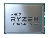
AMD is planning to surprise Intel by unveiling its 3rd generation Ryzen Threadripper HEDT (high-end desktop) processor lineup around the same time Intel launches its 10th generation Core "Cascade Lake-X" processor and the "Glacial Falls" HEDT platform, according to sources in the motherboard industry, speaking with DigiTimes. We're fairly sure the sources aren't referring to AMD's 16-core Ryzen 9 3950X processor, because it has already been announced and will be available in September.

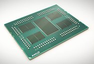
The 3rd generation Ryzen Threadripper will likely be a derivative of the company's "Rome" multi-chip module, and compatible with existing socket TR4 motherboards with a BIOS update, although a new chipset could also be launched to enable PCI-Express gen 4.0. AMD has the option to deploy up to 64 CPU cores across eight 7 nm "Zen 2" chiplets, while the 12 nm I/O controller die will be likely reconfigured for the HEDT platform with a monolithic 4-channel DDR4 memory interface and 64 PCIe gen 4.0 lanes. It's capable of 8 memory channels on the 2nd generation EPYC.

ZOTAC Rolls Out a Low-profile GeForce GTX 1650 Graphics Card

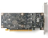
ZOTAC rolled out its first low-profile GeForce GTX 1650 graphics card, close to a month after MSI released the very first card of its kind. ZOTAC's 16 cm-long card uses a 2-slot thick chunky aluminium heatsink to cool the GPU, memory, and a portion of the VRM. This heatsink is ventilated by two 40 mm fans. The card relies on the PCI-Express slot for all its power, and runs the GPU at NVIDIA-reference clock speeds of 1665 MHz boost, and 8 Gbps GDDR5 memory. The card uses 4 GB of memory across a 128-bit wide memory bus. Based on the 12 nm "TU117" silicon, the GTX 1650 packs 896 CUDA cores, 56 TMUs, and 32 ROPs. Display outputs include one each of HDMI, DisplayPort, and DVI-D. The company didn't reveal pricing.

NVIDIA GeForce RTX 2080 Super Features 10 Percent Faster Memory

NVIDIA's upcoming GeForce RTX 2080 Super graphics card doesn't just max out the 12 nm "TU104" silicon and add higher GPU clock-speeds, but also features the highest-clocked GDDR6 memory solution on the market, to make the most of the 256-bit wide memory bus of the silicon. NVIDIA deployed 15.5 Gbps GDDR6 memory, which is 10.7 percent faster than the 14 Gbps memory used on the original RTX 2080 and other RTX 20-series graphics cards. The memory real-clock is set at 1937 MHz compared to 1750 MHz on the original RTX 2080. At this memory frequency, the RTX 2080 Super enjoys a memory bandwidth just a touch short of 500 GB/s, at 496 GB/s.

Besides memory, the RTX 2080 Super maxes out the "TU104" silicon by enabling all 3,072 CUDA cores physically present, as opposed to just 2,944 of them being enabled on the original RTX 2080. The card is also endowed with 192 TMUs, 64 ROPs, 384 Tensor cores, and 48 RT cores. The GPU frequencies are set at 1650 MHz with 1815 MHz GPU Boost, compared to 1515/1710 MHz of the original RTX 2080. NVIDIA is launching the RTX 2080 Super at an MSRP of USD $699, with availability slated for July 23. The company's add-in card (AIC) partners are allowed to design custom-design cards that come with improved cooling solutions and higher clocks.

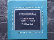
NVIDIA Manufacturing Turing GPUs at Samsung Korea Fab, 11nm?

During our disassembly of the GeForce RTX 2060 Super, we noticed a shocking detail. The 12 nm "TU106" GPU on which it is based, has the marking "Korea." We know for a fact that TSMC does not have any fabs there. The only Korean semiconductor manufacturer capable of contract-manufacturing a piece of silicon as complex as a GPU, for a designer with the energy-efficiency OCD as NVIDIA, is Samsung.

What makes this interesting is that Samsung does not officially have a 12 nm FinFET process. It has 14 nm, and the 11LPP, a 11 nm nodelet, which the company designed to compete with TSMC 12 nm. It would hence be really interesting to hear from NVIDIA on whether they've scaled out the "TU106" to 14LPP, or down to 11LPP at Samsung. It's interesting to note that the shrink in transistor sizes in these nodelets doesn't affect die-sizes. We hence see no die-size difference between these Korea-marked chips, and those marked "Taiwan." We've reached out to NVIDIA for comment.

Update July 3rd: NVIDIA got back to us
NVIDIAThe answer is really simple and these markings are not new. Other Turing GPUs have had these markings in the past. The chip is made at TSMC, but packaged in various locations. This one was done in Korea, hence why his says "Korea".

On an unrelated note: We already use both TSMC and Samsung, and qualify each of them for every process node. We can't comment in any further detail on future plans, but both remain terrific partners.

AMD Ryzen 3000 "Matisse" I/O Controller Die 12nm, Not 14nm

AMD Ryzen 3000 "Matisse" processors are multi-chip modules of two kinds of dies - one or two 7 nm 8-core "Zen 2" CPU chiplets, and an I/O controller die that packs the processor's dual-channel DDR4 memory controller, PCI-Express gen 4.0 root-complex, and an integrated southbridge that puts out some SoC I/O, such as two SATA 6 Gbps ports, four USB 3.1 Gen 2 ports, LPCIO (ISA), and SPI (for the UEFI BIOS ROM chip). It was earlier reported that while the Zen 2 CPU core chiplets are built on 7 nm process, the I/O controller is 14 nm. We have confirmation now that the I/O controller die is built on the more advanced 12 nm process, likely GlobalFoundries 12LP. This is the same process on which AMD builds its "Pinnacle Ridge" and "Polaris 30" chips. The 7 nm "Zen 2" CPU chiplets are made at TSMC.

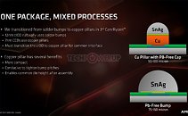
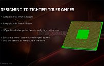
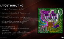
AMD also provided a fascinating technical insight to the making of the "Matisse" MCM, particularly getting three highly complex dies under the IHS of a mainstream-desktop processor package, and perfectly aligning the three for pin-compatibility with older generations of Ryzen AM4 processors that use monolithic dies, such as "Pinnacle Ridge" and "Raven Ridge." AMD innovated new copper-pillar 50µ bumps for the 8-core CPU chiplets, while leaving the I/O controller die with normal 75µ solder bumps. Unlike with its GPUs that need high-density wiring between the GPU die and HBM stacks, AMD could make do without a silicon interposer or TSVs (through-silicon-vias) to connect the three dies on "Matisse." The fiberglass substrate is now "fattened" up to 12 layers, to facilitate the inter-die wiring, as well as making sure every connection reaches the correct pin on the µPGA.

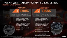
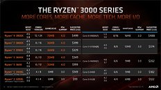
AMD Ryzen 3 3200G and Ryzen 5 3400G Detailed: New Slide Leak

At the bottom end of AMD's rather tall new Ryzen 3000 desktop processor product-stack are the Ryzen 3 3200G and Ryzen 5 3400G APUs. Unlike the rest of the Ryzen 3000 series, these two are based on the monolithic 12 nm "Picasso" silicon, which is essentially "Raven Ridge" redesigned for 12 nm with the "Zen+" microarchitecture. For the quad-core CPU, this means an improved Precision Boost algorithm that scales better across multiple cores, and faster on-die caches. For the iGPU based on the "Vega" architecture, this is a minor speed-bump.

The 3200G is configured with a 4-core/4-thread CPU and 8 out of 11 NGCUs of the iGPU enabled, yielding 512 stream processors. The maximum CPU clock speeds have been dialed up by 300 MHz over that of the 2200G, to now attain 4.00 GHz boost frequency, while the iGPU engine frequency is increased by 150 MHz, to 1250 MHz. The 3400G maxes out the silicon with a 4-core/8-thread CPU, and all 11 NGCUs enabled on the iGPU (704 stream processors). The CPU spools up to 4.20 GHz, and the iGPU up to 1400 MHz. AMD is including a bigger Wraith Spire cooling solution with the 3400G. Prices remain unchanged over the previous generation, with the 3200G being priced at USD $99, and the 3400G at $149, when the processors likely go on sale this July.

AMD Ryzen "Picasso" APU Clock Speeds Revealed

AMD is giving finishing touches to its Ryzen 3000 "Picasso" family of APUs, and Thai PC enthusiast TUM_APISAK has details on their CPU clock speeds. The Ryzen 3 3200G comes with 3.60 GHz nominal clock-speed and 4.00 GHz maximum Precision Boost frequency; while the Ryzen 5(?) 3400G ships with 3.70 GHz clock speeds along with 4.20 GHz max Precision Boost. The "Picasso" silicon is an optical shrink of the 14 nm "Raven Ridge" silicon to the 12 nm FinFET process at GlobalFoundries, the same one on which AMD builds "Pinnacle Ridge" and "Polaris 30."

Besides the shrink to 12 nm, "Picasso" features upgraded "Zen+" CPU cores that have improved Precision Boost algorithm and faster on-die caches, which contribute to a roughly 3% increase in IPC on "Pinnacle Ridge," but significantly improved multi-threaded performance compared to 1st generation Ryzen. Clock speeds of both the CPU cores and the integrated "Vega" iGPU are expected to increase. Both the 3200G and 3400G see a 100 MHz increase in nominal clock-speed, and 300 MHz increase in boost clocks, over the chips they succeed, the 2200G and 2400G, respectively. The iGPU is rumored to receive a similar 100-200 MHz increase in engine clock.

Lenovo Launches New ThinkPad Laptops Based on New AMD Ryzen PRO processors

Lenovo has released a trio of new Windows 10 laptops based on new, 2nd generation AMD Ryzen PRO processors, in their famous ThinkPad form factor. There are two models that are part of the T series of ThinkPads, while one is part of X series. For reminding, the T series is the flagship line that offers the best balance between ruggedness, features, processing power, and portability in a 14 or 15-inch unit, while the X series focuses on portability.

The new ThinkPads use the second generation of AMD Ryzen PRO processors, which are 12nm improvements of the previous 14nm Ryzen Family. They carry the 3000 name branding but are similar to the 2000 series of desktop CPUs.

NVIDIA GeForce GTX 1650 Released: TU117, 896 Cores, 4 GB GDDR5, $150

NVIDIA today rolled out the GeForce GTX 1650 graphics card at USD $149.99. Like its other GeForce GTX 16-series siblings, the GTX 1650 is derived from the "Turing" architecture, but without RTX real-time raytracing hardware, such as RT cores or tensor cores. The GTX 1650 is based on the 12 nm "TU117" silicon, which is the smallest implementation of "Turing." Measuring 200 mm² (die area), the TU117 crams 4.7 billion transistors. It is equipped with 896 CUDA cores, 56 TMUs, 32 ROPs, and a 128-bit wide GDDR5 memory interface, holding 4 GB of memory clocked at 8 Gbps (128 GB/s bandwidth). The GPU is clocked at 1485 MHz, and the GPU Boost at 1665 MHz.

The GeForce GTX 1650 at its given price is positioned competitively with the Radeon RX 570 4 GB from AMD. NVIDIA has been surprisingly low-key about this launch, by not just leaving it up to the partners to drive the launch, but also sample reviewers. There are no pre-launch Reviewer drivers provided by NVIDIA, and hence we don't have a launch-day review for you yet. We do have GTX 1650 graphics cards, namely the Palit GTX 1650 StormX, MSI GTX 1650 Gaming X, and ASUS ROG GTX 1650 Strix OC.

Update: Catch our reviews of the ASUS ROG Strix GTX 1650 OC and MSI GTX 1650 Gaming X

AMD Ryzen 3 3200G Pictured and De-lidded

AMD Ryzen 3 3200G is an upcoming processor featuring integrated graphics, forming the tail-end of the company's 3rd generation Ryzen desktop processor family. A Chinese PC enthusiast with access to an early sample pictured and de-lidded the processor. We know from older posts that while the "Matisse" MCM will form the bulk of AMD's 3rd gen Ryzen lineup, with core counts ranging all the way from 6 to 12, and possibly 16 later, the APU lineup is rumored to be based on older "Zen+" architecture.

The Ryzen 3 3200G and possibly the Ryzen 5 3400G, will be based on a derivative of the "Raven Ridge" silicon built on the 12 nm process at GlobalFoundries, and comes with a handful innovations AMD introduced with "Pinnacle Ridge," such as an improved Precision Boost algorithm and faster on-die caches. The 12 nm shrink also allows AMD to dial up CPU and iGPU engine clock speeds, and improve DDR4 memory support to work with higher DRAM clock speeds. AMD has used thermal paste as the sub-IHS interface material instead of solder for its "Raven Ridge" chips, and the story repeats with the 3200G.

NVIDIA GeForce GTX 1650 Specifications and Price Revealed

NVIDIA is releasing its most affordable graphics card based on the "Turing" architecture, the GeForce GTX 1650, on the 23rd of April, starting at USD $149. There doesn't appear to be a reference-design (the GTX 1660 series lacked one, too), and so this GPU will be a partner-driven launch. Based on NVIDIA's smallest "Turing" silicon, the 12 nm "TU117," the GTX 1650 will pack 896 CUDA cores and will feature 4 GB of GDDR5 memory across a 128-bit wide memory interface.

The GPU is clocked at 1485 MHz with 1665 MHz GPU Boost, and the 8 Gbps memory produces 128 GB/s of memory bandwidth. With a TDP of just 75 Watts, most GTX 1650 cards will lack additional PCIe power inputs, relying entirely on the slot for power. Most entry-level implementations of the GTX 1650 feature very simple aluminium fan-heatsink coolers. VideoCardz compiled a number of leaked pictures of upcoming GTX 1650 graphics cards.

AMD Readies 50th Anniversary Special Edition Ryzen 7 2700X

AMD is celebrating its 50th Anniversary with a new commemorative special edition package of the Ryzen 7 2700X eight-core desktop processor. This package carries the PIB SKU number "YD270XBGAFA50." American online retailer ShopBLT had it listed for USD $340.95 before pulling the listing down and marking it "out of stock." The listing doesn't come with any pictures or details about the SKU, except mentioning that a Wraith Prism RGB CPU cooler is included (as it normally is for the 2700X PIB package).

Given that AMD hasn't changed the model number, we expect these processors to have the same specifications as regular Ryzen 7 2700X, but with some special packaging material, and perhaps some special laser engraving on the processor's IHS. AMD has used tin boxes in the past for its first FX-series processors, so the possibility of something similar cannot be ruled out. Since pricing of this SKU isn't significantly higher, we don't expect it to be of a higher bin (better overclockers) than regular 2700X chips. Based on the 12 nm "Pinnacle Ridge" silicon, the 2700X is an 8-core/16-thread processor derived from the "Zen+" architecture, with 3.70 GHz clock-speed, 4.30 GHz maximum Precision Boost, XFR, L2 cache of 512 KB per core, and 16 MB of shared L3 cache.

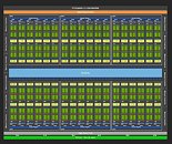
NVIDIA RTX Logic Increases TPC Area by 22% Compared to Non-RTX Turing

Public perception on NVIDIA's new RTX series of graphics cards was sometimes marred by an impression of wrong resource allocation from NVIDIA. The argument went that NVIDIA had greatly increased chip area by adding RTX functionality (in both its Tensor ad RT cores) that could have been better used for increased performance gains in shader-based, non-raytracing workloads. While the merits of ray tracing oas it stands (in terms of uptake from developers) are certainly worthy of discussion, it seems that NVIDIA didn't dedicate that much more die area to their RTX functionality - at least not to the tone of public perception.

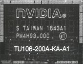
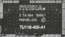
After analyzing full, high-res images of NVIDIA's TU106 and TU116 chips, reddit user @Qesa did some analysis on the TPC structure of NVIDIA's Turing chips, and arrived at the conclusion that the difference between NVIDIA's RTX-capable TU106 compared to their RTX-stripped TU116 amounts to a mere 1.95 mm² of additional logic per TPC - a 22% area increase. Of these, 1.25 mm² are reserved for the Tensor logic (which accelerates both DLSS and de-noising on ray-traced workloads), while only 0.7 mm² are being used for the RT cores.

AMD Announces 2nd Gen Ryzen PRO Mobile and Athlon PRO Mobile Processor Series

Today, AMD announced the latest additions to its PRO processor lineup: 2nd Gen AMD Ryzen PRO mobile processors with Radeon Vega Graphics and AMD Athlon PRO mobile processors with Radeon Vega Graphics. Providing commercial notebook users with power-efficient performance, state-of-the-art security features, and commercial-grade reliability and manageability, these new processors enable global PC manufacturers to create a wide range of business systems, from premium professional notebooks to everyday productivity notebooks. Initial commercial systems from HP and Lenovo are expected this quarter with other OEMs and further platform updates anticipated later in 2019.

"Modern PC users expect the experience between professional and personal to be imperceptible, and business notebook users want to utilize the latest modern features including 3D modeling, video editing, multi-display setups while multitasking securely, to get more done," said Saeid Moshkelani, senior vice president and general manager, Client Compute, AMD. "With AMD Ryzen PRO and Athlon PRO mobile processors, AMD delivers the right performance, features, and choice to OEMs and commercial users, combined with the productivity, protection, and professional features needed to ensure seamless deployment throughout an organization."

AMD "Cato" SoCs Figure in Futuremark SystemInfo

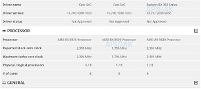
AMD could be giving finishing touches to its new generation of embedded SoCs codenamed "Cato." The chips surfaced on screenshots of UL Benchmarks (Futuremark) SystemInfo, across three models: the RX-8125, the RX-8120, and the A9-9820. For the uninitiated, the RX series embedded processors are part of the company's Ryzen Embedded family. The RX-series are differentiated from the A-series either by microarchitecture, or lack of unlocked multipliers, or other features, such as integrated graphics.

"Cato" is shrouded in mystery. One possible explanation could be AMD manufacturing the existing "Raven Ridge" IP on its refined 12 nm process, and "Zen+" enhancements to its CPUs. SystemInfo reading 8 logical processors could be a case of a 4-core/8-thread CPU configuration with SMT enabled. Another theory pegs this to be a new silicon, based on new IP, and 8 CPU cores. This is less probable since AMD is less stingy with SMT across its product-stack, and is hence less likely to deprive an 8-core silicon of SMT. If the latter theory is true, then this could simply be a case of the SystemInfo module not correctly detecting the prototype chips.

NVIDIA GeForce GTX 1650 Availability Revealed

NVIDIA is expected to launch its sub-$200 GeForce GTX 1650 graphics card on the 22nd of April, 2019. The card was earlier expected to launch towards the end of April. With it, NVIDIA will introduce the 12 nm "TU117," its smallest GPU based on the "Turing" architecture. The GTX 1650 could replace the current GTX 1060 3 GB, and may compete with AMD offerings in this segment, such as the Radeon RX 570 4 GB, in being Full HD-capable if not letting you max your game settings out at that resolution. The card could ship with 4 GB of GDDR5 memory.

NVIDIA GeForce GTX 1650 Details Leak Thanks to EEC Filing

The GeForce GTX 1650 will be NVIDIA's smallest "Turing" based graphics card, and is slated for a late-April launch as NVIDIA waits on inventories of sub-$200 "Pascal" based graphics cards, such as the GTX 1050 series, to be digested by the retail channel. A Eurasian Economic Commission filing revealed many more details of this card, as an MSI Gaming X custom-design board was finding its way through the regulator. The filing confirms that the GTX 1650 will pack 4 GB of memory. The GPU will be based on the new 12 nm "TU117" silicon, which will be NVIDIA's smallest based on the "Turing" architecture. This card will likely target e-Sports gamers, giving them the ability to max out their online battle royale titles at 1080p. It will probably compete with AMD's Radeon RX 570.

NVIDIA Launches the GeForce GTX 1660 6GB Graphics Card

NVIDIA today launched the GeForce GTX 1660 6 GB graphics card, its successor to the immensely popular GTX 1060 6 GB. With prices starting at $219.99, the GTX 1660 is based on the same 12 nm "TU116" silicon as the GTX 1660 Ti launched last month; with fewer CUDA cores and a slower memory interface. NVIDIA carved the GTX 1660 out by disabling 2 out of 24 "Turing" SMs on the TU116, resulting in 1,408 CUDA cores, 88 TMUs, and 48 ROPs. The company is using 8 Gbps GDDR5 memory instead of 12 Gbps GDDR6, which makes its memory sub-system 33 percent slower. The GPU is clocked at 1530 MHz, with 1785 MHz boost, which are marginally higher than the GTX 1660 Ti. The GeForce GTX 1660 is a partner-driven launch, meaning that there won't be any reference-design cards, although NVIDIA made should every AIC partner has at least one product selling at the baseline price of $219.99.

Read TechPowerUp Reviews: Zotac GeForce GTX 1660 | EVGA GeForce GTX 1660 XC Ultra | Palit GeForce GTX 1660 StormX OC | MSI GTX 1660 Gaming X

Update: We have updated our GPU database with all GTX 1660 models announced today, so you can easily get an overview over what has been released.

EVGA and GIGABYTE GeForce GTX 1660 Graphics Cards Pictured

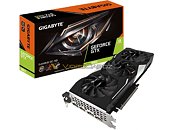
Here are some of the first pictures of EVGA's and GIGABYTE's upcoming GeForce GTX 1660 graphics cards reportedly slated for launch later this week. It should come as no surprise that these cards resemble the companies' GTX 1660 Ti offerings, since they're based on the same 12 nm "TU116" silicon, with fewer CUDA cores. The underlying PCBs could be slightly different as the GTX 1660 uses older generation 8 Gbps GDDR5 memory instead of 12 Gbps GDDR6. The "TU116" silicon is configured with 1,408 CUDA cores out of the 1,536 physically present; the memory amount is 6 GB, across a 192-bit wide memory bus. The GTX 1660 baseline price is reportedly USD $219, and the card replaces the GTX 1060 6 GB from NVIDIA's product stack.

EVGA is bringing two designs to the market, a short-length triple-slot card with a single fan; and a more conventional longer card with 2-slot, dual-fan design. The baseline "Black" card could be offered in the shorter design; while the top-tier XC Ultra could be exclusive to the longer design. GIGABYTE, on the other hand, has two designs, a shorter-length dual-fan; and a longer-length triple-fan. Both models are dual-slot. The baseline SKU will be restricted to the shorter board design, while premium Gaming OC SKUs could come in the longer board design.

GIGABYTE Rolls Out its Radeon RX 590 Gaming Graphics Card

That took a little while, but GIGABYTE has finally updated their lineup with an AMD RX 590 graphics card. Based on the 12 nm-revised Polaris 30 silicon with higher clocks than those that could be achieved by its 14 nm predecessors (already the RX 480 and RX 580 graphics cards), the GIGABYTE RX 590 Gaming rbings the already well-known 2304 Stream processors, and gets them to tick at 1560 MHz (against AMD's 1545 MHz reference). It's a usual GIGABYTE graphics card by all standards, with a dual-fan WindForce 2X cooling solution with fan-stop functionality.

It seems GIGABYTE finally went through some of that unsold RX inventory, and is now looking to keep the channel supplied until the next best thing from the red team makes its appearance (hopefully sooner rather than later.)

NVIDIA GeForce GTX 1660 and GTX 1650 Pricing and Availability Revealed

(Update 1: Andreas Schilling, at Hardware Luxx, seems to have obtained confirmation that NVIDIA's GTX 1650 graphics cards will pack 4 GB of GDDR5 memory, and that the GTX 1660 will be offering a 6 GB GDDR5 framebuffer.)

NVIDIA recently launched its GeForce GTX 1660 Ti graphics card at USD $279, which is the most affordable desktop discrete graphics card based on the "Turing" architecture thus far. NVIDIA's GeForce 16-series GPUs are based on 12 nm "Turing" chips, but lack RTX real-time ray-tracing and tensor cores that accelerate AI. The company is making two affordable additions to the GTX 16-series in March and April, according to Taiwan-based PC industry observer DigiTimes.

The GTX 1660 Ti launch will be followed by that of the GeForce GTX 1660 (non-Ti) on 15th March, 2019. This SKU is likely based on the same "TU116" silicon as the GTX 1660 Ti, but with fewer CUDA cores and possibly slower memory or lesser memory amount. NVIDIA is pricing the GTX 1660 at $229.99, a whole $50 cheaper than the GTX 1660 Ti. That's not all. We recently reported on the GeForce GTX 1650, which could quite possibly become NVIDIA's smallest "Turing" based desktop GPU. This product is real, and is bound for 30th April, at $179.99, $50 cheaper still than the GTX 1660. This SKU is expected to be based on the smaller "TU117" silicon. Much like the GTX 1660 Ti, these two launches could be entirely partner-driven, with the lack of reference-design cards.

NVIDIA Unveils the GeForce GTX 1660 Ti 6GB Graphics Card

NVIDIA today unveiled the GeForce GTX 1660 Ti graphics card, which is part of its new GeForce GTX 16-series product lineup based on the "Turing" architecture. These cards feature CUDA cores from the "Turing" generation, but lack RTX real-time raytracing features due to a physical lack of RT cores, and additionally lack tensor cores, losing out on DLSS. What you get instead with the GTX 1660 Ti is a upper-mainstream product that could play most eSports titles at resolutions of up to 1440p, and AAA titles at 1080p with details maxed out.

The GTX 1660 Ti is based on the new 12 nm "TU116" silicon, and packs 1,536 "Turing" CUDA cores, 96 TMUs, 48 ROPs, and a 192-bit wide memory interface holding 6 GB of GDDR6 memory. The memory is clocked at 12 Gbps, yielding 288 GB/s of memory bandwidth. The launch is exclusively partner-driven, and NVIDIA doesn't have a Founders Edition product based on this chip. You will find custom-design cards priced anywhere between USD $279 to $340.

We thoroughly reviewed four GTX 1660 Ti variants today: MSI GTX 1660 Ti Gaming X, EVGA GTX 1660 Ti XC Black, Zotac GTX 1660 Ti, MSI GTX 1660 Ti Ventus XS.

Gainward Announces its GeForce GTX 1660 Ti Series

As the leading brand in enthusiastic graphics market, Gainward proudly presents the all new GeForce GTX 1660 Ti series - Gainward GeForce GTX 1660 Ti Ghost and Gainward GeForce GTX 1660 Ti Pegasus series. Gainward's new GeForce GTX 1660 Ti series is built with the breakthrough graphics performance of the award-winning NVIDIA Turing architecture. These advanced graphics cards are designed to deliver a powerful combination of gaming innovation and next-gen graphics. With the new Turing's architecture, the gaming performance will outgo up to 1.5 times than the GeForce GTX 1060 6GB. It's a blazing-fast supercharger for today's most popular games, and even faster with modern titles.
Return to Keyword Browsing
Nov 21st, 2024 13:02 EST change timezone

New Forum Posts

Popular Reviews

Controversial News Posts