News Posts matching #BGA

Return to Keyword Browsing

AMD TSMC's Second Largest Customer for 5nm, More Resilient Than Intel to Face Downturns in the PC Industry: Report

AMD is now TSMC's second largest customer for its 5 nanometer N5 silicon fabrication node, according to a DigiTimes report. The Taiwan-based semiconductor industry observer also reports that AMD is more resilient than Intel in facing any downturns in the PC industry, in the coming few months. PC sales are expected to slump by as much as 15 percent in the near future, but the lower market-share compared to Intel; and the flexibility for AMD to move its CPU chips over to enterprise product to feed the growth in server processor segment, means that the company can ride over a bumpy road in the near future. The lower market-share translates to "lesser pain" from a slump compared to Intel. The report also says that embracing TSMC for processors "just in time" means that AMD has a front-row seat with product performance, time-to-market, yields, and delivery.

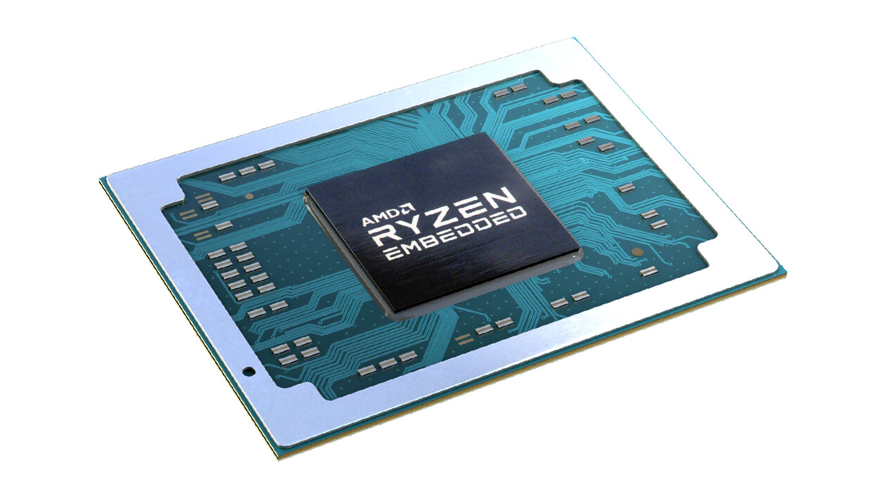
AMD is on the anvil of two major product launches on 5 nm, the Ryzen 7000 series "Raphael" desktop processors on August 30 (according to the report), and EPYC "Genoa" server processors in November 2022. The company is planning to refresh its notebook processor lineup in the first half of 2023, with "Dragon Range," and "Phoenix Point" targeting distinct market segments among notebooks. "Dragon Range" is essentially "Raphael" (5 nm chiplet + 6 nm cIOD) on a mobile-optimized BGA package, letting AMD cram up to 16 "Zen 4" cores, and take on Intel's high core-count mobile processors. The iGPU of "Dragon Range" will be basic, since designs based on this chip are expected to use discrete GPUs. "Phoenix Point" is a purpose-built mobile processor with up to 8 "Zen 4" cores, and a powerful iGPU based the RDNA3 architecture.

Winbond's LPDDR4/4X 100BGA achieves JEDEC standard for improved energy conservation and carbon reduction in a smaller package size

Winbond Electronics Corporation, a leading global supplier of semiconductor memory solutions, today announced that its new package 100BGA LPDDR4/4X had achieved the JEDEC JED209-4 standard to ensure energy conservation and carbon reduction. The LPDDR4/4X is now available in a space-saving 100BGA package measuring only 7.5X10mm2. The device is ideal for IoT applications requiring higher throughput in a small package to allow designers to reduce the PCB size for more compact IoT designs.

Winbond's LPDDR4/4X memory is available in density of 1Gb and 2Gb, supporting speeds of up to 4267 Mbps. It is available in both Single-Die-Package (SDP) with a 2Gb density and Dual-Die-Package (DDP) with a 4Gb density. The higher speed of LPDDR4 1CH x16 4267 Mbps offers improved performance over previous DDR4 x16 3200 Mbps devices, which is especially useful for consumer applications.

ATP Announces High-Endurance 3D TLC-based eMMC Devices

ATP Electronics, the global leader in specialized storage and memory solutions, has introduced its latest line of e.MMC devices built on 3D triple level cell (TLC) NAND. Using a new die package, the E750Pi/Pc and E650Si/Sc Series offer long-life performance, optimized power consumption and customizable configuration options. ATP's new E750Pi/Pc Series e.MMC offerings are built with 3D TLC NAND flash but are configured as pseudo SLC (pSLC) to offer endurance on par with SLC NAND, while E650Si/Sc Series in native TLC has near-MLC endurance.

The E750Pi and E650Si Series are industrial temperature-operable (-40°C to 85°C), making them ideal for deployment in scenarios with extreme thermal challenges and harsh environments, while E750Pc and E650Sc support -25°C to 85°C operating temperatures for applications with non-critical thermal requirements.

Fujitsu Launches New 8Mbit FRAM Guaranteeing Writing Endurance up to 100 Trillion Times

Fujitsu Semiconductor Memory Solution Limited has launched new 8 Mbit FRAM MB85R8M2TA with parallel interface, which is the first product to guarantee 100 trillion read/write cycle times in Fujitsu's FRAM product family. Evaluation samples are currently available. The new product achieves both high-speed operations, approximately 30% faster access speed, and low power consumption, 10% less operating current, compared to Fujitsu's conventional products. This memory IC is an ideal replacement of SRAM in the industrial machines that require high-speed operation.

FRAM is a non-volatile memory product with superior features of high read/write endurance, fast writing speed operation and low power consumption, and it has been mass-produced for over 20 years. Fujitsu has been providing 8 Mbit FRAM MB85R8M2T with parallel interface since June 2018. While promoting the product, the company heard voices of customer requirements such as guaranteed writing endurance of more than 10 trillion times, operation as fast as SRAM and TSOP package compatibility to SRAM. Fujitsu is now pleased to introduce its new 8 Mbit FRAM product satisfying these requirements, maintaining FRAM's unique feature of lower power consumption.

Longsys Launches FORESEE DDR4 DRAM Chips

With the rapid development of advanced technologies, such as 5G, the Internet of Things (IoT), Artificial Intelligence (AI), and 8K, people are placing more stringent requirements on the convenience, intelligence, and functional integration of their electronics. This has given rise to new development opportunities in the storage industry. As we progress further into the digital revolution, intelligent electronics will require small-capacity storage products which feature an increased level of reliability and stability. High-temperature tolerance in storage products will be vital for customers in the intelligent and small-sized consumer electronics market.

Longsys recently launched the FORESEE DDR4, which utilizes 96-ball thin fine ball grid array (TFBGA) encapsulation. The product's manufacturing process, transmission speed, power consumption, and high-temperature reliability all perform at an industry-leading level.

SkyHigh Memory expands its single-level cell (SLC) NAND Flash Memory family on 1xnm process technology, one of the industry's most advanced technology

SkyHigh Memory Limited., a global leader in embedded storage solutions, is introducing 3.0 V 1 Gb - 4 Gb densities 4 KB page and 2 KB page ML-3 products to its family of NAND Flash memories. The new 1 Gb - 4 Gb ML-3 SLC NAND Flash product family devices are designed on 1xnm, the industry's most advanced technology node for SLC NAND products. Available with different interfaces, SkyHigh Memory first-generation Serial (SPI) SLC NAND and third-generation Parallel SLC NAND complete the third generation ML-3 4 Gb - 16 Gb parallel SLC NAND product family already in production.

The new 1 Gb - 4 Gb devices will be offered to support high-reliability systems that store critical data and operate at extended temperatures, up to +105°C. Thanks to its internal ECC engine, the ML-3 product family can support chipsets with as low as a 1-bit ECC engine to accommodate legacy chipsets and modern chipsets with higher ECC engines.

AMD Ryzen Embedded V3000 SoCs Based on 6nm Node, Zen 3 Microarchitecture

AMD's next generation Ryzen Embedded V3000 system-on-chips aren't simply "Cezanne" dies sitting on BGA packages, but rather based on a brand new silicon, according to Patrick Schur, a reliable source with leaks. The die will be built on the more advanced 6 nm silicon fabrication node, whilst still being based on the current "Zen 3" microarchitecture. There are several things that set it apart from the APU silicon of the current-generation, making it more relevant for the applications the Ryzen Embedded processor family is originally built for.

Built in the FP7r2 BGA package, the V3000 silicon features an 8-core/16-thread CPU based on the "Zen 3" microarchitecture. There are also an integrated GPU based on the RDNA2 graphics architecture, with up to 12 CUs, a dual-channel DDR5 memory interface, a 20-lane PCI-Express 4.0 root complex, with up to 8 lanes put out for PEG; two USB4 ports, and two 10 GbE PHYs. AMD could design at least three SKUs based on this silicon, spanning TDP bands of 15-30 W and 35-54 W.

Intel NUC 11 Extreme "Beast Canyon" to Feature KB CPUs - Desktop Power, Mobile Socket

Intel's NUC 11 Extreme, codenamed Beast Canyon, is a revisit - and in some terms, reimagining - of the Extreme performance NUC range by Intel. The new Beast Canyon NUCs will now support full-length discrete graphics cards as well Intel's compute element in a single, 8L compact case. The compute element, which we have already pictured before, has now been photographed up close, manifesting one of Intel's latest additions to its ARK database - the NUC features a Core i9-11900KB CPU.

Intel has registered four B-line CPUs on its Ark: the i9-11900KB (unlocked, mobile socket, NUC-bound); i7-11700B; i5-11500B; and i3-11100B. All of these CPUs are meant for the NUC form-factor, are part of Intel's Next Unit of Computing design, and will ship in an add-in card form factor which already includes the socketed, mobile CPU (likely in BGA packaging), the RAM sticks, storage subsystem, and I/O complex. It remains to be seen whether this new form-factor convinces those interested in such a system - the added capability to add full-length PCIe graphics cards may add some flexibility, but it does come at the expense of physical footprint for the new generation NUC.

Intel Xe-HPG DG2 GPU Specifications Leak, First GPUs are Coming in H2 2021 in Alder Lake-P Laptops

Yesterday, we got information that Intel's upcoming DG2 discrete graphics card is "right around the corner". That means that we are inching closer to the launch of Intel's discrete GPU offerings, and we are going to get another major player in the current GPU market duopoly. Today, however, we are in luck because Igor from Igor's LAB has managed to get ahold of the specifications of Intel's Xe-HPG DG2 graphics card. For starters, it is important to note that DG2 GPU will first come to laptops later this year. More precisely, laptops powered by Alder Lake-P processors will get paired with DG2 discrete GPU in the second half of 2021. The CPU and GPU will connect using the PCIe 4.0 x12 link as shown in the diagram below, where the GPU is paired with the Tiger Lake-H processor. The GPU has its subsystem that handles the IO as well.

ATP Launches PCIe Gen3 x4 NVMe SSDs in M.2 Type 1620 HSBGA Package

ATP Electronics, the global leader in specialized storage and memory solutions, has announced the launch of its tiniest NVMe flash storage offering: the N700 Series PCIe Gen3 x4 NVMe solid state drives (SSDs, which are available as M.2 Type 1620 heatsink ball-grid array (HSBGA) package. Complying with M.2 specifications, the M.2 Type 1620 HSBGA measures just 16 (L) x 20 (W) x 1.6 (H) mm, supporting high-speed PCIe 3.0 interface x4 lanes and NVMe protocol to deliver up to 32 Gb/s bandwidth at 8 Gb/s per lane. The soldered-down design makes them vibration-proof, while the 291-ball packaging takes up minimal space within tightly confined systems.

For customers who prefer a removable and field-replaceable design, ATP can accommodate the HSBGA onto an M.2 2230 module with the same firmware and NAND configuration. Both variants are suitable for thin and light systems in embedded, industrial and mobile applications. N700 Series SSDs are built with 3D triple-level cell (TLC) configured as pseudo single-level cell (pSLC) NAND flash. By storing only one bit per cell, they increase the reliability and endurance of the NAND flash memory, while benefiting from the lower cost compared with native SLC, due to the higher cell density.

Greenliant Ultra High Endurance Storage Solutions Enable High Reliability Systems

Greenliant has secured major design wins with its EnduroSLC solid state drives (SSDs) in a wide range of demanding, extreme environment applications for customers that need best-in-class reliability and product longevity. Greenliant's proprietary EnduroSLC Technology substantially enhances data retention and extends the write endurance of 1-bit-per-cell SSDs with advanced hardware ECC capabilities and NAND flash management algorithms. EnduroSLC SSDs not only offer superior data retention capabilities under complex temperature conditions, but also support 50K, 100K and industry-leading, ultra high 250K+ program-erase (P/E) cycles, which are at least a 5x improvement over pseudo-SLC (pSLC) SSDs and a 50x improvement over MLC NAND-based products.

For systems that are in remote locations and costly to maintain-from satellite to subsea communications-customers recognize the value of EnduroSLC SSDs; they can reliably operate and retain data for long periods of time in harsh conditions. Long-life, write-intensive products, such as transportation black box recorders and industrial data loggers, have also benefitted from the enhanced features of EnduroSLC SSDs. EnduroSLC storage products are designed with Greenliant's advanced SATA, NVMe PCIe and eMMC controllers, operate at industrial temperatures (-40 to +85 degrees Celsius) and are backed by the company's Long-Term Availability program (http://bit.ly/SSD-LTA-program), providing an extra level of support.

Intel Confirms Development of 8-core Tiger Lake-H Processors

Intel's Corporate Vice President of Client Computing Group Boyd Phelps posted an article on medium where he confirms development of 8-core Tiger Lake-based CPU solutions, to be released during the year 2021. This was confirmed by Boyd saying that 8-core Tiger Lake CPUs would have access to 24 MB of LLC cache (adequately doubling the 12 MB available for 4-core Tiger Lake-U parts that we already know about); Boyd then simply added in parentheticals "more detail on 8-core products at a later date".

The 8-core processors will be part of the Tiger Lake-H product stack, which, according to a leaker on PTT Shopping, would scale between the 35 W-45 W TDPs with various core and GPU Execution Unit counts. The 45 W high-performance parts can feature between 4, 6, and 8-cores - but additional space taken up by the CPU cores is thus unavailable for GPU resources, which top out at 32 Intel Xe EUs (and will make use of a BGA1787 socket). The 35 W variants, on the other hand, will be installed in the same socket as Tiger Lake-U - BGA 1449 - and reportedly only offer a 4-core design with 96 EUs.

Penguin Computing Packs 7616 Intel Xeon Platinum Cores in one Server Rack

In data centers of hyperscalers like Amazon, Google, Facebook, and ones alike, there is a massive need for more computing power. Being that data centers are space-limited facilities, it is beneficial if there is a system that can pack as much computing power as possible, in a smaller form factor. Penguin Computing has thought exactly about this problem and has decided to launch a TundraAP platform, designed specifically as a high-density CPU system. Using an Intel Xeon Platinum 9200 processor, the company utilizes Intel's processor with the highest core count - 56 cores spread on two dies, brought together by a single BGA package.

The Penguin Computing TundraAP system relies on Intel's S9200WK server system. In a 1U server, Penguin Computing puts two of those in one system, with a twist. The company implements a power disaggregation system, which is designed to handle and remove the heat coming from those 400 W TPD monster processors. This means that the PSU is moved from the server itself and moved on a special rack, so the heat from the CPUs wouldn't affect PSUs. The company uses Open Compute Project standards and says it improves efficiency by 15%. To cool those chips, Penguin Computing uses a direct-to-chip liquid cooling system. And if you are wondering how much cores the company can fit in a rack, look no further as it is possible to have as much as 7616 Xeon Platinum cores in just one rack. This is a huge achievement as the density is quite big. The custom cooling and power delivery system that the company built enabled this, by only allowing compute elements to be present in the system.

AMD and Industry Partners to Develop New Blockchain-based Gaming Platforms

AMD today announced that it has joined the Blockchain Game Alliance (BGA) and forged partnerships with leading technology providers to help promote the development and proliferation of new blockchain-powered gaming platforms.

The Blockchain Game Alliance is committed to driving awareness and adoption of blockchain technologies within the game industry, providing an open forum for individuals and companies to share knowledge and collaborate, create common standards, establish best practices, and network. As the first major hardware manufacturer to join the BGA, AMD plans to enable alliance members with efficient and high-performance computing technologies for next-generation blockchain-based gaming platforms that could potentially transform the way games are created, published, purchased and played.

Memory Chip Swap Mod SUPERcharges an RTX 2080 Ti

Overclocking the memory clock of a GeForce RTX 2080 Ti to 2000 MHz (16 Gbps) isn't difficult, but most custom-design RTX 2080 Ti cards cap out at that, and so the enthusiasts over at TecLab took matters into their own hands by pulling off a daring memory chip replacement mod, by installing 16 Gbps-rated memory chips onto a Galax RTX 2080 Ti HOF graphics card. In a 16-minute video presentation, they detail the process of soldering a component as delicate and sensitive as GDDR6 memory chips, and 45 times over. The team had to sacrifice not one, but two Galax GeForce RTX 2080 Super graphics cards, which feature 16 Gbps-rated memory chips to support the SKU's 15.5 Gbps memory clock. A total of 33 manual solder operations had to be performed (removing the 15 stock chips from the RTX 2080 Ti, removing 11 chips from the two RTX 2080 Super cards, and soldering them onto the RTX 2080 Ti).

The group detailed the process of removing the memory chips under hot air, giving the extracted chips fresh ball-grids, and placing the chips onto the RTX 2080 Ti PCB. No BIOS modding was required, as the RTX 2080 Ti card's video BIOS was able to auto-detect the chips and run them at 14 Gbps. From here on, manual overclocking easily runs the card at 2000 MHz (16 Gbps) memory, with overclocking headroom to spare. The memory clock could now be dialed all the way up to 2150 MHz (17.2 Gbps), something that's close to impossible with 14 Gbps chips. TecLab is calling their creation the world's first RTX 2080 Ti Super, which could very well be true. Last we heard, the RTX 2080 Ti Super could get more CUDA cores, and not just faster memory. Nevertheless, this mod blew our minds, and provides valuable pointers on how to solder dense BGA components without a multi million-dollar placer. We tip our hats to TecLab.
Watch the TechLab video presentation here.

Greenliant ArmourDrive SSDs Reach 250,000+ P/E Cycles with EnduroSLC Technology

Greenliant is now sampling its new high-reliability SATA 6 Gb/s ArmourDrive EX Series products to customers that need ultra robust data retention, ultra high endurance data storage capable of operating under heavy workloads in extreme environments. Designed with Greenliant's EnduroSLC Technology, SATA ArmourDrive EX Series solid state storage modules achieve 50K, 100K and industry-leading 250K+ program-erase (P/E) cycles and provide enhanced data retention. EnduroSLC-enabled SSDs offer high data storage integrity and can withstand wide temperature operations without losing data.

The SATA ArmourDrive EX Series expands the EnduroSLC product family, which also includes SATA 6Gb/s NANDrive and 100-ball/153-ball eMMC NANDrive ball grid array (BGA) solid state drives (SSDs). "SSD and memory card users that need super-high endurance and long-term data retention over a broad temperature range have limited options, since today's NAND flash marketplace is highly focused on consumer applications," said Jim Handy, principal analyst, Objective Analysis. "Greenliant's EnduroSLC products should find a warm reception among these elite users."

Greenliant Offers Superior Data Retention and Endurance with EnduroSLC SATA NANDrive SSDs

Greenliant is now sampling its SATA 6Gb/s NANDrive EX Series ball grid array (BGA) solid state drives (SSDs) to customers that require superior data retention and high program-erase (P/E) cycles. Designed with Greenliant's EnduroSLC Technology, SATA 6 Gb/s NANDrive EX Series SSDs are capable of performing 50K, 100K and industry-leading 250K+ P/E cycles. EnduroSLC Technology substantially enhances data retention and extends write endurance of 1-bit-per-cell (SLC) SSDs with advanced hardware ECC capabilities and NAND flash management algorithms.

Developed with Greenliant's DRAM-less controller, SATA 6 Gb/s NANDrive has enhanced power loss data protection and offers four times the performance over the previous generation of SATA NANDrive products. SATA 6 Gb/s SSDs support Native Command Queuing (NCQ) up to 32 commands and use advanced NAND management techniques to optimize the device's performance during its lifetime. With faster read/write speeds and available in a wide range of capacities (2 GB - 128 GB), SATA 6 Gb/s NANDrive EX Series is ideal for high-performance computing, industrial, transportation, video and networking applications.

Marvell Announces 88SS1320-series PCIe Gen4 NVMe SSD Controllers

Marvell today released the industry's lowest power PCIe Gen4 NVMe solid-state drive (SSD) controller portfolio. Marvell's newest SSD controllers are designed to meet the need for lower power and higher performance in next-generation data centers and edge devices as artificial intelligence (AI) and 5G gain momentum. This breakthrough technology delivers unparalleled performance in an ultra-compact footprint, leveraging the company's complex system-on-chip (SoC) design expertise and groundbreaking storage IP to help data center, notebook, tablet, gaming and edge computing platform architects advance their solutions for the highly distributed data era.

"Marvell's latest family of storage controllers has been architected to optimally address edge computing and data center pain points of power-performance and capacity-performance," said Nigel Alvares, vice president of marketing for the Flash Business Unit at Marvell Semiconductor, Inc. "With today's launch, we're once again demonstrating Marvell's leadership in storage, delivering the industry's first 4-Channel PCIe Gen4 NVMe SSD controllers with the industry's lowest power consumption that will help revolutionize SSD solutions for the data economy."

ADATA Announces IUSP33F PCIe BGA SSD

ADATA Technology, a leading manufacturer of high-performance DRAM modules and NAND flash products, today launched the ADATA IUSP33F PCIe ball grid array (BGA) solid state drive (SSD). The SSD sports a form factor that is 80 percent more compact than M.2 2242 SSDs. Combined with a PCIe Gen3x2 interface and 3D Flash memory for excellent performance and durability, the IUSP33F is an ideal solution for slim-form-factor tablets, notebooks, hybrids, mini-PCs, thin clients, and wearables.

"We are thrilled to be introducing the new IUSP33F SSD, a compact solution that will enable next-generation tablets, ultrabooks, and other slim devices, but without compromising on performance and reliability," said Hedi Huang, Sales Directorof ADATA. "But the versatility of the IUSP33F goes beyond just these applications, and are also well-suited for new emerging applications in areas such as robotics, augmented and virtual reality, and automotive.

ATP Announces eMMC 5.1 Chips

Fueled by continuous big data generation, the ongoing industrial revolution requires storage solutions that offer not only high performance, but also uncompromising reliability and maximum endurance. ATP Electronics, a leading manufacturer of industrial memory and storage solutions, tackles these tough storage demands with its new industrial e.MMC product family.

The ATP industrial e.MMC, which adheres to JEDEC e.MMC v5.1 Standard (JESD84-B51), is poised to make its mark at the Flash Memory Summit 2018 in Santa Clara, USA from August 7 to 9, 2018.

Intel's 8th Gen Core-B Processors Are BGA Solutions for AIOs

Intel has announced, in-between the flurry of announcement sin the past week, that they're introducing a line of BGA (Ball-Grid Array) microprocessors to their 8th Gen line-up with the Core-B branding. The new CPUs look to deliver easily installed, scalable, premium processor options for all sorts of limited Z-height computing packages, such as the ones found in AIOs, without sacrificing performance in order to keep TDPs in check.

This means that these processors ship with a 65W TDP - higher than Intel's top-performing mobile H solutions. This move may come in handy for some users that wonder regarding upgradeability of a given AIO they're eyeing - if it comes with a Core-B processor, you know it won't be user-serviceable, much less upgradeable. The line-up will start with the Core i7-8700B, i5-8500B, and i5-8400 (yes, there's an absence of a B there) processors, all shipping with a 65 W TDP, and equivalent to their desktop counterparts - core counts, base frequencies, turbo frequencies, memory support, Optane support, and integrated graphics are all the same. The only difference is that these CPUs are likely - and should be expected - to be placed into TDP-limited scenarios enabled through firmware.
Return to Keyword Browsing
Jul 3rd, 2025 02:58 CDT change timezone

New Forum Posts

Popular Reviews

TPU on YouTube

Controversial News Posts