News Posts matching #Die

Return to Keyword Browsing

Apple A14 SoC Put Under the Microscope; Die Size, and Transistor Density Calculated

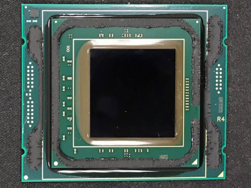
Apple has established itself as a master of silicon integrated circuit design and has proven over the years that its processors deliver the best results, generation after generation. If we take a look at the performance numbers of the latest A14 Bionic, you can conclude that its performance is now rivaling some of the x86_64 chips. So you would wonder, what is inside this SoC that makes it so fast? That is exactly what ICmasters, a semiconductor reverse engineering and IP services company, has questioned and decided to find out. For starters, we know that Apple manufactures the new SoCs on TSMC's N5 5 nm node. The Taiwanese company promises to pack 171.3 million transistors per square millimeter, so how does it compare to an actual product?

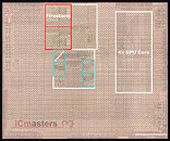
ICmasters have used electron microscopy to see what the chip is made out of and to measure the transistor density. According to this source, Apple has a chip with a die size of 88 mm², which packs 11.8 billion N5 transistors. The density metric, however, doesn't correspond to that of TSMC. Instead of 171.3 million transistors per mm², the ICmasters measured 134.09 million transistors per mm². This is quite a difference, however, it is worth noting that each design will have it different due to different logic and cache layout.
Apple A14 SoC Die Apple A14 SoC

Samsung Starts Offering First A-Die Based RAM

Samsung's B die has been widely known as a good, high performance variant of DRAM memory, loved by overclockers because of its ability to get to a high frequency with relatively low timings. However, B die has been discontinued and now Samsung started offering its replacement in form of the newly developed A die manufactured in 1z nm (1z class) lithography process. Despite the lack of technical details surrounding the new die type, Hardwareluxx has received a tip from its reader about new RAM offering that incorporates A die memory.

The M378A4G43AB2-CVF, as it is called in the listing, is a 32 GB, single dimm DDR4 RAM with operating speed of 2933 MHz and CL21-21-21 timings. This particular offer isn't something to be excited about as the frequency is good, but the timings are quite high for that speed. Given that we don't know where the A die is targeted at, we can speculate that its current aim is at mid-tier systems, where the mediocre performance is okay and the system isn't suffering (performance wise) because of it. Nonetheless this find is quite interesting as it gives first hints at what can we expect in therms of future A die DRAM offerings. Remember, it took some time for B die as well to get to the level of performance we have today, so it is entirely possible that A die will improve and try to aim for greater performance level than it currently has.

Samsung Launches Sixth Generation 3D V-NAND SSDs

Samsung Electronics, the world leader in advanced memory technology, today announced that it has begun mass producing 250-gigabyte (GB) SATA solid state drive (SSD) that integrates the company's sixth-generation (1xx-layer) 256-gigabit (Gb) three-bit V-NAND for global PC OEMs. By launching a new generation of V-NAND in just 13 months, Samsung has reduced the mass production cycle by four months while securing the industry's highest performance, power efficiency and manufacturing productivity.

"By bringing cutting-edge 3D memory technology to volume production, we are able to introduce timely memory lineups that significantly raise the bar for speed and power efficiency," said Kye Hyun Kyung, executive vice president of Solution Product & Development at Samsung Electronics. "With faster development cycles for next-generation V-NAND products, we plan to rapidly expand the markets for our high-speed, high-capacity 512 Gb V-NAND-based solutions."

Samsung Kills Production of Famed B-die DDR4 Memory in Favor or Higher Densities

As the world becomes more and more centered on data, as well as its processing and storage, increased memory density across products is becoming more of a necessity. It seems that out of this necessity and a need to streamline its memory production towards favoring denser outputs, Samsung is killing of the famous B-die chips, which were - and still are - part of a love affair with any enthusiast's Ryzen desktop.

Memory compatibility issues with the first gen Ryzen took a while to dissipate, and didn't vanish entirely; however, overclockers quickly found that the most stable and overclockable memory ICs all were of the Samsung B-die type. Now, the company has updated its product catalogue to reflect EOL (End of Life) status for B-dies, replacing it with denser M-Die and A-Die products. M-dies were supposed to bring 32 GB densities to a single rank of memory - and have apparently been siphoned off to server applications and left out in the cold for consumer purchase), while the new A dies increase memory density per IC, meaning less of these are necessary to achieve the same final memory footprint. Whether or not these will feature the same Ryzen compatibility and overclockability as their B-die predecessors is unknown at this point, but it would make a lot of enthusiasts slightly unhappy - and increase the value of B-die offerings in any sort of discerning second-hand market - if they did not.

The Ncore V1 is the World's First Naked Die Cooling Waterblock for LGA1151 CPUs

The world's first waterblock designed for naked die cooling throws years of conventional wisdom out of the window. It features six unique patentable features including its "in-frame" mounting mechanism. The man behind NUDEcnc, Arek Tobiszewski has started this Kickstarter campaign in order to get a professional CNC machine, which will enable this inventor to deliver Ncore and other cool projects to the audience. He has been brave enough to send the Ncore for a review to Kyle Bennett from HardOcp; Linus tech tips; buildzoid, and Techlipton. Some of the reviews are already up, and are very promising.

Intel Skylake-X HCC CPU Delidded by Der8auer, also not Soldered

Overclocking poster-boy Der8auer has seemingly gotten his hands on some early samples of Intel's Skylake-X high core count (HCC)HEDT CPUs. The upcoming 12 to 18-core enthusiast-class CPUs are being launched on the same X299 platform on socket LGA 2066 that Intel has already launched 4 (Kaby Lake-X), 6, 8 and 10-core parts already, and are supposed to bring Intel towards a level playing field - and then some - with competitor AMD's Threadripper CPUs, which boast of up to 16 cores.

From this delidding process with Der8auer's own delidding tool, Delid-Die-Mate-X, seems to result a die that is much larger - as expected - than Intel's 10-core i9-7900X. At the same time, it seems that Intel is still opting, again, for not soldering its enthusiast-targeted CPUs, which would result in better temperatures and, potentially, overclocking potential. The fact that Der8auer managed to delid the i9-7920X and didn't recommend against doing it likely means that there is minimal risk of damaging your CPU while subjecting it to this process. This is something the renowned overclocker did do when he recommended that users shouldn't delid their Ryzen or Threadripper CPUs looking for better temperatures, since the fact that these were soldered would likely result in both catastrophic damage and a much diminished chance of operating temperatures improvement through the application of special purpose thermal compounds. The Facebook post from Der8auer with the delidded 7920X likely serves as an appetizer for an upcoming delid video on YouTube, as has been the overclocker's MO.

AMD Raja Koduri Confirms RX Vega Die Size at 484 mm²

AMD's Raja Koduri, leader of the company's Radeon Technologies Group, has somewhat informally confirmed on Twitter the overall die size of AMD's Vega chips. After PC Perspective updated their prognosis regarding Vega's die-size to a beefier 512 mm², Twitter users plied Raja Koduri with questions regarding this subject. Koduri declined to answer directly, actually opting for a somewhat cryptic response, in that " (...) the answer [to Vega's die-size] is the closest perfect square number actually:)".

For the math-savvy around here (or even just for those of you who have read the headline), that particular equation should solve towards a perfect 484 mm² die area. Good news for AMD: this isn't the company's biggest die-size in consumer GPUs ever. That dubious honor goes to the company's Fiji XT silicon which powered the company's R9 Fury X, coming in at a staggering 596 mm² in the 28 nm process. For comparison, AMD's current Polaris 20 XTX-based RX 580 chip comes in at slightly less than half the confirmed RX Vega's die-size, at a much more yield-friendly 232 mm². NVIDIA's current top-of-the-line Titan Xp comes in at a slightly smaller 471 mm² die-size.
Return to Keyword Browsing
Jul 13th, 2025 04:50 CDT change timezone

New Forum Posts

Popular Reviews

TPU on YouTube

Controversial News Posts