TSMC: 5 nm on Track for Q2 2020 HVM, Ramping Faster than 7 nm
TSMC vice chairman and CEO C.C. Wei announced the company's plans for 5 nm are on track, which means High Volume manufacturing (HVM) on the node is expected to be achieved by 2Q 2020. The company has increased expenditures in ramping up its various nodes from an initially projected $10 billion to something along the lines of $14 billion - 15 billion; the company is really banking on quick uptake and design wins on its most modern process technologies - and the increased demand that follows.
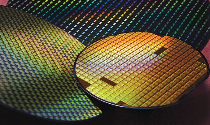
TSMC's 5 nm process (N5) will use extreme ultraviolet lithography (EUVL) in many more layers than its N7+ and N6 processes, with up to 14 layers being etched in the N5 silicon compared to five and six, respectively, for its "older" N7+ and N6 processes. As the company increases capital expenditure in acquiring EUVL-capable equipment that sets up its production nodes for the market they foresee will just gobble up the chips in 2020, the company is optimistic they can achieve growth in the 5-10% number.
TSMC's 5 nm process (N5) will use extreme ultraviolet lithography (EUVL) in many more layers than its N7+ and N6 processes, with up to 14 layers being etched in the N5 silicon compared to five and six, respectively, for its "older" N7+ and N6 processes. As the company increases capital expenditure in acquiring EUVL-capable equipment that sets up its production nodes for the market they foresee will just gobble up the chips in 2020, the company is optimistic they can achieve growth in the 5-10% number.