News Posts matching #GA102

Return to Keyword Browsing

ASUS ROG Strix GeForce RTX 3090 Ampere Pictured

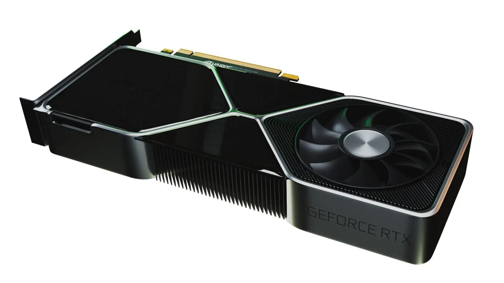
Here's a much clearer picture of the ROG Strix GeForce RTX 3090 "Ampere" graphics card by ASUS. A render of this card was revealed back in July, when the RTX 3090 was still speculated to be called the "RTX 3080 Ti." The card features the latest iteration of the ROG Strix design scheme by ASUS, with more shiny metal bits that conceal lighting elements. The cooler features a chunky aluminium fin-stack heatsink that's ventilated by three Axial-Tech fans. The card is 3 slots thick, and about an inch taller than what would constitute "full height." VideoCardz, which is also the source of the image, predicts that ASUS could use same board design for both the RTX 3090 and the RTX 3080. We've seen custom-design RTX 3090 cards featuring as many as three 8-pin PCIe power inputs, while those based on the RTX 3080 have been shown with two. With the RTX 3090 and RTX 3080 being based on the common silicon, the GA102, differing in memory and core configurations, the R&D costs for custom-design board partners is greatly reduced.

NVIDIA GeForce RTX 3090 and 3080 Specifications Leaked

Just ahead of the September launch, specifications of NVIDIA's upcoming RTX Ampere lineup have been leaked by industry sources over at VideoCardz. According to the website, three alleged GeForce SKUs are being launched in September - RTX 3090, RTX 3080, and RTX 3070. The new lineup features major improvements: 2nd generation ray-tracing cores and 3rd generation tensor cores made for AI and ML. When it comes to connectivity and I/O, the new cards use the PCIe 4.0 interface and have support for the latest display outputs like HDMI 2.1 and DisplayPort 1.4a.

The GeForce RTX 3090 comes with 24 GB of GDDR6X memory running on a 384-bit bus at 19.5 Gbps. This gives a memory bandwidth capacity of 936 GB/s. The card features the GA102-300 GPU with 5,248 CUDA cores running at 1695 MHz, and is rated for 350 W TGP (board power). While the Founders Edition cards will use NVIDIA's new 12-pin power connector, non-Founders Edition cards, from board partners like ASUS, MSI and Gigabyte, will be powered by two 8-pin connectors. Next up is specs for the GeForce RTX 3080, a GA102-200 based card that has 4,352 CUDA cores running at 1710 MHz, paired with 10 GB of GDDR6X memory running at 19 Gbps. The memory is connected with a 320-bit bus that achieves 760 GB/s bandwidth. The board is rated at 320 W and the card is designed to be powered by dual 8-pin connectors. And finally, there is the GeForce RTX 3070, which is built around the GA104-300 GPU with a yet unknown number of CUDA cores. We only know that it has the older non-X GDDR6 memory that runs at 16 Gbps speed on a 256-bit bus. The GPUs are supposedly manufactured on TSMC's 7 nm process, possibly the EUV variant.

NVIDIA Ampere GA102-300-A1 GPU Die Pictured

Here's the first picture of an NVIDIA "Ampere" GA102 GPU die. This is the largest client-segment implementation of the "Ampere" architecture by NVIDIA, targeting the gaming (GeForce) and professional-visualization (Quadro) market segments. The "Ampere" architecture itself debuted earlier this year with the A100 Tensor Core scalar processor that's winning hearts and minds in the HPC community faster than ice cream on a dog day afternoon. There's no indication of die-size, but considering how tiny the 10.3 billion-transistor AMD "Navi 10" die is, the GA102 could come with a massive transistor count if its die is as big as that of the TU102. The GPU in the picture is also a qualification sample, and was probably pictured off a prototype graphics card. Powering the GeForce RTX 3090, the GA102-300 is expected to feature a CUDA core count of 5,248. According to VideoCardz, there's a higher trim of this silicon, the GA102-400, which could make it to NVIDIA's next halo product under the TITAN brand.

Video Memory Sizes Set to Swell as NVIDIA Readies 20GB and 24GB GeForce Amperes

NVIDIA's GeForce RTX 20-series "Turing" graphics card series did not increase video memory sizes in comparison to GeForce GTX 10-series "Pascal," although the memory itself is faster on account of GDDR6. This could change with the GeForce RTX 30-series "Ampere," as the company looks to increase memory sizes across the board in a bid to shore up ray-tracing performance. WCCFTech has learned that in addition to a variety of strange new memory bus widths, such as 320-bit, NVIDIA could introduce certain higher variants of its RTX 30-series cards with video memory sizes as high as 20 GB and 24 GB.

Memory sizes of 20 GB or 24 GB aren't new for NVIDIA's professional-segment Quadro products, but it's certainly new for GeForce, with only the company's TITAN-series products breaking the 20 GB-mark at prices due north of $2,000. Much of NVIDIA's high-end appears to be resting on segmentation of the PG132 common board design, coupled with the GA102 silicon, from which the company could carve out several SKUs spaced far apart in the company's product stack. NVIDIA's next-generation GeForce "Ampere" family is expected to debut in September 2020, with product launches in the higher-end running through late-Q3 and Q4 of 2020.

NVIDIA GeForce "Ampere" GPUs Built on Samsung 8nm Instead of TSMC 7nm?

NVIDIA's upcoming GeForce "Ampere" family of GPUs will be built almost entirely on Samsung's 8 nanometer silicon fabrication process that's derived from its 10 nm node; rather than TSMC's 7 nm process, according to kopite7kimi, a source with a high hit-rate with NVIDIA rumors in the past. The 8LPP silicon fabrication node by Samsung is an extension of the company's 10LPP (10 nm) node. Both have the same fin pitch, but reductions are made in the areas of gate pitch (down by 6%) resulting in a transistor density of over 61 million/mm². Apparently NVIDIA's entire high-end product stack, including the GA102 silicon that powers at least three high-end consumer SKUs, are expected to be based on Samsung 8LPP.

NVIDIA's Next-Gen Reference Cooler Costs $150 By Itself, to Feature in Three SKUs

Pictures of alleged next-generation GeForce "Ampere" graphics cards emerged over the weekend, which many of our readers found hard to believe. It's features a dual-fan cooling solution, in which one of the two fans is on the reverse side of the card, blowing air outward from the cooling solution, while the PCB extends two-thirds the length of the card. Since then, there have been several fan-made 3D renders of the card. NVIDIA is not happy with the leak, and started an investigation into two of its contractors responsible for manufacturing Founders Edition (reference design) GeForce graphics cards, Foxconn and BYD (Build Your Dreams), according to a report by Igor's Lab.

According to the report, the cooling solution, which looks a lot more overengineered than the company's RTX 20-series Founders Edition cooler, costs a hefty USD $150, or roughly the price of a 280 mm AIO CLC. It wouldn't surprise us if Asetek's RadCard costs less. The cooler consists of several interconnected heatsink elements with the PCB in the middle. Igor's Lab reports that the card is estimated to be 21.9 cm in length. Given its cost, NVIDIA is reserving this cooler for only the top three SKUs in the lineup, the TITAN RTX successor, the RTX 2080 Ti successor, and the RTX 2080/SUPER successor.

NVIDIA RTX 3080 Ti and GA102 "Ampere" Specs, Other Juicy Bits Revealed

PC hardware focused YouTube channel Moore's Law is Dead published a juicy tech-spec reveal of NVIDIA's next-generation "Ampere" based flagship consumer graphics card, the GeForce RTX 3080 Ti, citing correspondence with sources within NVIDIA. The report talks of big changes to NVIDIA's Founders Edition (reference) board design, as well as what's on the silicon. To begin with, the RTX 3080 Ti reference-design card features a triple-fan cooling solution unlike the RTX 20-series. This cooler is reportedly quieter than the RTX 2080 Ti FE cooling solution. The card pulls power from a pair of 8-pin PCIe power connectors. Display outputs include three DP, and one each of HDMI and VirtualLink USB-C. The source confirms that "Ampere" will implement PCI-Express gen 4.0 x16 host interface.

With "Ampere," NVIDIA is developing three tiers of high-end GPUs, with the "GA102" leading the pack and succeeding the "TU102," the "GA104" holding the upper-performance segment and succeeding today's "TU104," but a new silicon between the two, codenamed "GA103," with no predecessor from the current-generation. The "GA102" reportedly features 5,376 "Ampere" CUDA cores (up to 10% higher IPC than "Turing"). The silicon also taps into the rumored 7 nm-class silicon fabrication node to dial up GPU clock speeds well above 2.20 GHz even for the "GA102." Smaller chips in the series can boost beyond 2.50 GHz, according to the report. Even with the "GA102" being slightly cut-down for the RTX 3080 Ti, the silicon could end up with FP32 compute performance in excess of 21 TFLOPs. The card uses faster 18 Gbps GDDR6 memory, ending up with 863 GB/s of memory bandwidth that's 40% higher than that of the RTX 2080 Ti (if the memory bus width ends up 384-bit). Below are screengrabs from the Moore's Law is Dead video presentation, and not NVIDIA slides.
Return to Keyword Browsing
Feb 3rd, 2025 19:01 EST change timezone

New Forum Posts

Popular Reviews

Controversial News Posts