Monday, May 11th 2020

NVIDIA RTX 3080 Ti and GA102 "Ampere" Specs, Other Juicy Bits Revealed
PC hardware focused YouTube channel Moore's Law is Dead published a juicy tech-spec reveal of NVIDIA's next-generation "Ampere" based flagship consumer graphics card, the GeForce RTX 3080 Ti, citing correspondence with sources within NVIDIA. The report talks of big changes to NVIDIA's Founders Edition (reference) board design, as well as what's on the silicon. To begin with, the RTX 3080 Ti reference-design card features a triple-fan cooling solution unlike the RTX 20-series. This cooler is reportedly quieter than the RTX 2080 Ti FE cooling solution. The card pulls power from a pair of 8-pin PCIe power connectors. Display outputs include three DP, and one each of HDMI and VirtualLink USB-C. The source confirms that "Ampere" will implement PCI-Express gen 4.0 x16 host interface.
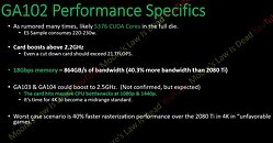
With "Ampere," NVIDIA is developing three tiers of high-end GPUs, with the "GA102" leading the pack and succeeding the "TU102," the "GA104" holding the upper-performance segment and succeeding today's "TU104," but a new silicon between the two, codenamed "GA103," with no predecessor from the current-generation. The "GA102" reportedly features 5,376 "Ampere" CUDA cores (up to 10% higher IPC than "Turing"). The silicon also taps into the rumored 7 nm-class silicon fabrication node to dial up GPU clock speeds well above 2.20 GHz even for the "GA102." Smaller chips in the series can boost beyond 2.50 GHz, according to the report. Even with the "GA102" being slightly cut-down for the RTX 3080 Ti, the silicon could end up with FP32 compute performance in excess of 21 TFLOPs. The card uses faster 18 Gbps GDDR6 memory, ending up with 863 GB/s of memory bandwidth that's 40% higher than that of the RTX 2080 Ti (if the memory bus width ends up 384-bit). Below are screengrabs from the Moore's Law is Dead video presentation, and not NVIDIA slides.As for performance, the "GA102" based prototype is allegedly clocking 40 percent higher performance than the RTX 2080 Ti at 4K UHD resolution in poorly optimized games, 50% higher performance on optimized games, and up to 70 percent performance in the "best case scenario" (a game that's been optimized for the "Ampere" architecture). We know from older leaks that by increasing the number of streaming multiprocessors, NVIDIA is doubling the CUDA core : RT core ratio compared to Turing, resulting in more RT cores per tier; and increased ray-tracing performance.
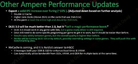
Each "Ampere" RT core is able to process 4x more intersections per unit clock-speed than "Turing." The tensor core count is also reportedly going to see an increase. The focus on ray-tracing and AI performance increase could give game developers the freedom to cram in more RTX effects per title, letting users disable what they want on older "Turing" cards. Performance limitations on "Turing" made developers choose from the RTX feature-set on what to implement. With "Ampere," NVIDIA could introduce DLSS 3.0, an updated image quality and performance enhancement. NVIDIA could resurrect a hybrid memory technology similar to AMD's HBCC, called NVCache, which spreads video memory across the video memory, the system memory, and flash-based storage.Lastly, there's more clarity as to what silicon fabrication process NVIDIA could use. Apparently, NVIDIA will spread its product stack between two kinds of 7 nm-class nodes. The higher-end ASICs, such as the "GA102" and "GA103," could be built on 7 nm EUV nodes such as the TSMC N7+; while the smaller ASICs could be built on conventional DUV-based 7 nm-class nodes such as the N7P or even N7.
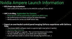
Don't pull your wallets out just yet. The launch schedule points to May 2020 (GTC) being focused on HPC parts based on "Ampere," such as the Tesla A100 and DGX A100 system.
In September 2020, NVIDIA will hold a separate event specifically to launch the next-generation GeForce, very close to "Cyberpunk 2077" release.
Source:
Moore's Law is Dead (YouTube)
With "Ampere," NVIDIA is developing three tiers of high-end GPUs, with the "GA102" leading the pack and succeeding the "TU102," the "GA104" holding the upper-performance segment and succeeding today's "TU104," but a new silicon between the two, codenamed "GA103," with no predecessor from the current-generation. The "GA102" reportedly features 5,376 "Ampere" CUDA cores (up to 10% higher IPC than "Turing"). The silicon also taps into the rumored 7 nm-class silicon fabrication node to dial up GPU clock speeds well above 2.20 GHz even for the "GA102." Smaller chips in the series can boost beyond 2.50 GHz, according to the report. Even with the "GA102" being slightly cut-down for the RTX 3080 Ti, the silicon could end up with FP32 compute performance in excess of 21 TFLOPs. The card uses faster 18 Gbps GDDR6 memory, ending up with 863 GB/s of memory bandwidth that's 40% higher than that of the RTX 2080 Ti (if the memory bus width ends up 384-bit). Below are screengrabs from the Moore's Law is Dead video presentation, and not NVIDIA slides.As for performance, the "GA102" based prototype is allegedly clocking 40 percent higher performance than the RTX 2080 Ti at 4K UHD resolution in poorly optimized games, 50% higher performance on optimized games, and up to 70 percent performance in the "best case scenario" (a game that's been optimized for the "Ampere" architecture). We know from older leaks that by increasing the number of streaming multiprocessors, NVIDIA is doubling the CUDA core : RT core ratio compared to Turing, resulting in more RT cores per tier; and increased ray-tracing performance.
Each "Ampere" RT core is able to process 4x more intersections per unit clock-speed than "Turing." The tensor core count is also reportedly going to see an increase. The focus on ray-tracing and AI performance increase could give game developers the freedom to cram in more RTX effects per title, letting users disable what they want on older "Turing" cards. Performance limitations on "Turing" made developers choose from the RTX feature-set on what to implement. With "Ampere," NVIDIA could introduce DLSS 3.0, an updated image quality and performance enhancement. NVIDIA could resurrect a hybrid memory technology similar to AMD's HBCC, called NVCache, which spreads video memory across the video memory, the system memory, and flash-based storage.Lastly, there's more clarity as to what silicon fabrication process NVIDIA could use. Apparently, NVIDIA will spread its product stack between two kinds of 7 nm-class nodes. The higher-end ASICs, such as the "GA102" and "GA103," could be built on 7 nm EUV nodes such as the TSMC N7+; while the smaller ASICs could be built on conventional DUV-based 7 nm-class nodes such as the N7P or even N7.
Don't pull your wallets out just yet. The launch schedule points to May 2020 (GTC) being focused on HPC parts based on "Ampere," such as the Tesla A100 and DGX A100 system.
In September 2020, NVIDIA will hold a separate event specifically to launch the next-generation GeForce, very close to "Cyberpunk 2077" release.


83 Comments on NVIDIA RTX 3080 Ti and GA102 "Ampere" Specs, Other Juicy Bits Revealed
"new control panel merged with geforce experience" Ho boy. Some people are going to be so mad about that.
Still really interested in RDNA2 as well it sounded a lot like AMD was going to do sort of a single PCB dual chip GPU and make it more of a standardized GPU for the entire generation of GPU's? Unless I interpreted what I had read in some article on it wrong I only read one article that hinted toward that kind of thing, but I could be wrong about that I haven't kept close tabs on it overall other than some tid bits on about RNDA2 to do with consoles. I'd expect more from Nvidia this generation than AMD for GPU's personally given they are doing a die shrink, but who knows. It's a interesting time for GPU's especially with all the flexibility of the added PCIe 4.0 bandwidth to work with.
The 10 & 12 GB cards (3080/3080Ti) are going to be fine but if midrange cards such as the 3070 only get 8GB it's going to be disappointing.
I don't think 8GB is going to cut it long-term.
I hope nvidia gives more options with more VRAM, I would pay an extra 100$ for the 16GB Version of the 70 class Card.
4x better RT performance doesn't necessarily mean 4x higher framerates when RT is enabled, it could mean 4x faster HW acceleration which at the end should give different results depending on the workload, so don't expect some magic to happen. The Performance cost of Ray Tracing is not going anywhere, it could be reduced but not completely eliminated.
..and if it does turn out to be the case, It says more about how poor the first generation of RT cards are/were, than it says about how good Ampere might be.
We all know what Intel did....or rather did not do due to lack of competition.
ALso I know it does not matter but I do find it kinda boring the most high end unit in this segment not using HBM memory.yeah, but probably....bout 500 dollar pls
The 1080 > 3070 jump will already likely be significant, RT is bonus. 1080 > 3080 will be over 50%. I'm also pretty optimistic about the ratio / increase of RT, it was clear something had to give, the balance seems alright. Its also clear they use DLSS to make room for that in terms of performance. Overall I get the impression Nvidia is holding on to their performance increase in rasterized ops per gen. Very nice. This makes RT 'just bonus'.
And this is what I meant when I said 'Just wait' when Turing dropped. Its nice RDNA2 is going to compete. Thanks, AMD.
RTX 2080 Ti doesn't need 3 power connectors.
2 x 8-pin is good for 75 + 2 x 150 watts.
- 4x better Ray Tracing performance
- Global illumination, shadows and reflections all at the same time
- Higher core clocks (Above 2GHz)
September is going to be a proper time to upgrade for sure!
7nm should be more efficient bringing the TDP down, so why the double 8 pin and tripple fan design.
With Turing Nvidia made a mess with 1660 and 2060, so it was pretty hard to tell where the actual mid-range was/is. I don't imagine this separation will be there with Ampere.