Monday, May 11th 2020

NVIDIA RTX 3080 Ti and GA102 "Ampere" Specs, Other Juicy Bits Revealed
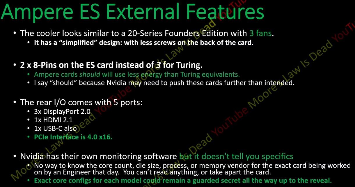
PC hardware focused YouTube channel Moore's Law is Dead published a juicy tech-spec reveal of NVIDIA's next-generation "Ampere" based flagship consumer graphics card, the GeForce RTX 3080 Ti, citing correspondence with sources within NVIDIA. The report talks of big changes to NVIDIA's Founders Edition (reference) board design, as well as what's on the silicon. To begin with, the RTX 3080 Ti reference-design card features a triple-fan cooling solution unlike the RTX 20-series. This cooler is reportedly quieter than the RTX 2080 Ti FE cooling solution. The card pulls power from a pair of 8-pin PCIe power connectors. Display outputs include three DP, and one each of HDMI and VirtualLink USB-C. The source confirms that "Ampere" will implement PCI-Express gen 4.0 x16 host interface.
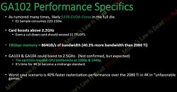
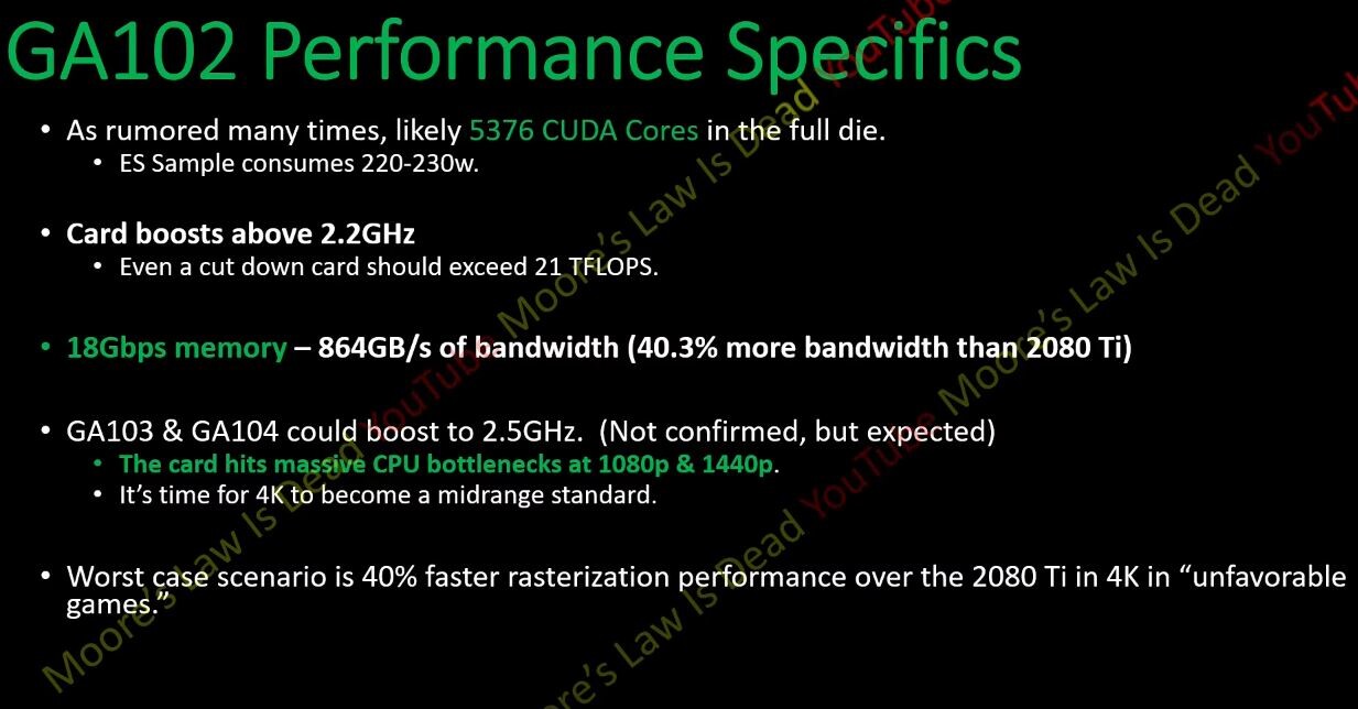
With "Ampere," NVIDIA is developing three tiers of high-end GPUs, with the "GA102" leading the pack and succeeding the "TU102," the "GA104" holding the upper-performance segment and succeeding today's "TU104," but a new silicon between the two, codenamed "GA103," with no predecessor from the current-generation. The "GA102" reportedly features 5,376 "Ampere" CUDA cores (up to 10% higher IPC than "Turing"). The silicon also taps into the rumored 7 nm-class silicon fabrication node to dial up GPU clock speeds well above 2.20 GHz even for the "GA102." Smaller chips in the series can boost beyond 2.50 GHz, according to the report. Even with the "GA102" being slightly cut-down for the RTX 3080 Ti, the silicon could end up with FP32 compute performance in excess of 21 TFLOPs. The card uses faster 18 Gbps GDDR6 memory, ending up with 863 GB/s of memory bandwidth that's 40% higher than that of the RTX 2080 Ti (if the memory bus width ends up 384-bit). Below are screengrabs from the Moore's Law is Dead video presentation, and not NVIDIA slides.
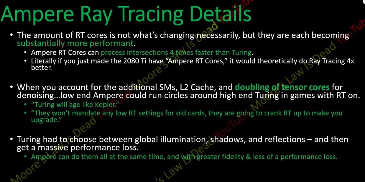
 As for performance, the "GA102" based prototype is allegedly clocking 40 percent higher performance than the RTX 2080 Ti at 4K UHD resolution in poorly optimized games, 50% higher performance on optimized games, and up to 70 percent performance in the "best case scenario" (a game that's been optimized for the "Ampere" architecture). We know from older leaks that by increasing the number of streaming multiprocessors, NVIDIA is doubling the CUDA core : RT core ratio compared to Turing, resulting in more RT cores per tier; and increased ray-tracing performance.
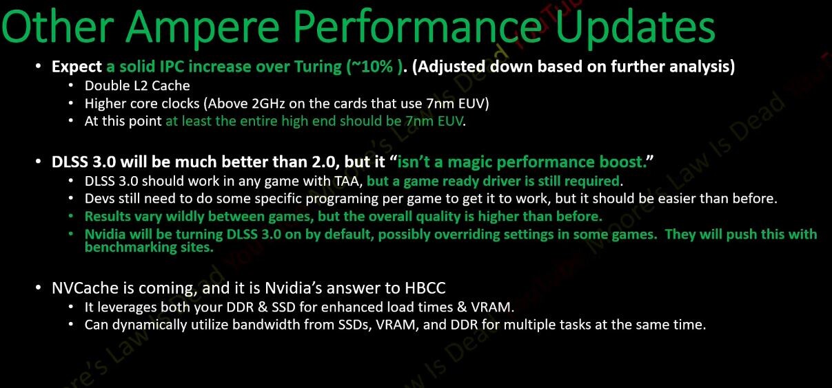
Each "Ampere" RT core is able to process 4x more intersections per unit clock-speed than "Turing." The tensor core count is also reportedly going to see an increase. The focus on ray-tracing and AI performance increase could give game developers the freedom to cram in more RTX effects per title, letting users disable what they want on older "Turing" cards. Performance limitations on "Turing" made developers choose from the RTX feature-set on what to implement. With "Ampere," NVIDIA could introduce DLSS 3.0, an updated image quality and performance enhancement. NVIDIA could resurrect a hybrid memory technology similar to AMD's HBCC, called NVCache, which spreads video memory across the video memory, the system memory, and flash-based storage.
 Lastly, there's more clarity as to what silicon fabrication process NVIDIA could use. Apparently, NVIDIA will spread its product stack between two kinds of 7 nm-class nodes. The higher-end ASICs, such as the "GA102" and "GA103," could be built on 7 nm EUV nodes such as the TSMC N7+; while the smaller ASICs could be built on conventional DUV-based 7 nm-class nodes such as the N7P or even N7.
Don't pull your wallets out just yet. The launch schedule points to May 2020 (GTC) being focused on HPC parts based on "Ampere," such as the Tesla A100 and DGX A100 system.
In September 2020, NVIDIA will hold a separate event specifically to launch the next-generation GeForce, very close to "Cyberpunk 2077" release.
Source:
Moore's Law is Dead (YouTube)
With "Ampere," NVIDIA is developing three tiers of high-end GPUs, with the "GA102" leading the pack and succeeding the "TU102," the "GA104" holding the upper-performance segment and succeeding today's "TU104," but a new silicon between the two, codenamed "GA103," with no predecessor from the current-generation. The "GA102" reportedly features 5,376 "Ampere" CUDA cores (up to 10% higher IPC than "Turing"). The silicon also taps into the rumored 7 nm-class silicon fabrication node to dial up GPU clock speeds well above 2.20 GHz even for the "GA102." Smaller chips in the series can boost beyond 2.50 GHz, according to the report. Even with the "GA102" being slightly cut-down for the RTX 3080 Ti, the silicon could end up with FP32 compute performance in excess of 21 TFLOPs. The card uses faster 18 Gbps GDDR6 memory, ending up with 863 GB/s of memory bandwidth that's 40% higher than that of the RTX 2080 Ti (if the memory bus width ends up 384-bit). Below are screengrabs from the Moore's Law is Dead video presentation, and not NVIDIA slides.
Each "Ampere" RT core is able to process 4x more intersections per unit clock-speed than "Turing." The tensor core count is also reportedly going to see an increase. The focus on ray-tracing and AI performance increase could give game developers the freedom to cram in more RTX effects per title, letting users disable what they want on older "Turing" cards. Performance limitations on "Turing" made developers choose from the RTX feature-set on what to implement. With "Ampere," NVIDIA could introduce DLSS 3.0, an updated image quality and performance enhancement. NVIDIA could resurrect a hybrid memory technology similar to AMD's HBCC, called NVCache, which spreads video memory across the video memory, the system memory, and flash-based storage.
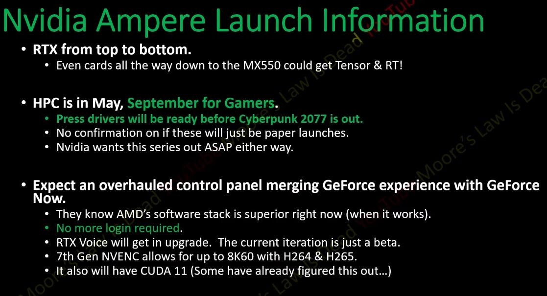
Don't pull your wallets out just yet. The launch schedule points to May 2020 (GTC) being focused on HPC parts based on "Ampere," such as the Tesla A100 and DGX A100 system.
In September 2020, NVIDIA will hold a separate event specifically to launch the next-generation GeForce, very close to "Cyberpunk 2077" release.
83 Comments on NVIDIA RTX 3080 Ti and GA102 "Ampere" Specs, Other Juicy Bits Revealed
Usually he speaks about things way in advance and then months later Wccftech or some other site makes a story about "breaking news". Hes was pretty spot on about the new console specs before others. When it comes to SMT4 - that may still come. But plans change and it's likely pushed back. If the SMT4 thing is the only one you can think of the id say that's quite good for a leak/speculation channel to get this one thing wrong.
Because the more time goes by, the more I begin to doubt that we will ever see a new generation :lol:
Anyone got any guesses on the cost of one of these 3080 Ti's?? Or have they mentioned a price??
3080Ti: 999
3080: 700
3070: 500
3060: 350
Just my guess. Remember that unless AMD prices their cards very close to Nvidia then Nvidia can't just ask whatever they want. They can't even tout RT as some exlusive feature. Nvidia overpriced Turing because they had no competition at the high end and they could say "hey look we are the only one who has RT". With RDNA2 they don't have that advantage. I think the bigger problem could be AMD's pricing.
When the new 70’s can squeak by we all celebrate that a low-high end/high midrange card can do it and what a great value that makes it. But it is not the normal way of it.
How many does nvidea have right now?
Introducing models 5% apart so they can charge more for less...
Nobody can actually like the Nvidia control panel as it is right now? It's poorly laid out, skinned for Windows XP and lacks features that AMD give that are either nice to have or downright mandatory IMO.
on.
- I've been using it since forever
- I open it so rarely. Basically never, the only times I used it was when I needed to change a game's profile. But I've stopped gaming.
I'm not opposed to change or added features, I'm just saying the current CP is not a sore spot for me.
First post on that page starts the discussion pertaining to this video.
HBCC and tensor-core-accelerated RAM compression are specifically called out as nonsense.
I was told it is at around 8%. Which makes it pretty much on par.No doubt about that, except this gen we might see Huang eat crow for messing with TSMC.The cakewalk NV had back in Raja times was based on total absence of AMD chips in major parts of the market, followed by very bad Vega metrics (big chip + expensive RAM and meh performance) which left high end to full throttle milking by Huang.
Now that gamers are trained to pay obnoxious sums for GPUs, what we'll see with next gen would hardly be a deathmatch. NV will milk a bit less, AMD will push it's ever raising margins closer to Intel/NV margins.
There will be no cutthroat competition.
Major technological gap between the two exists only in someone's imagination.
PS
It's not a gaming card.