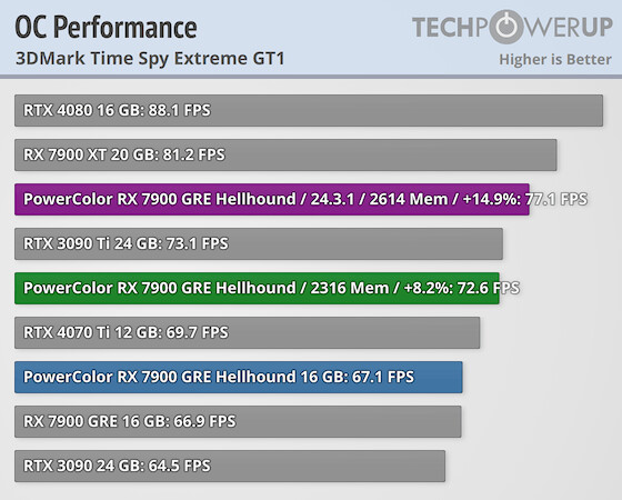
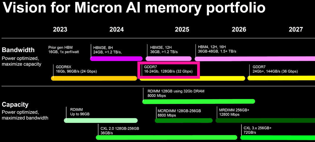
News Posts matching #GDDR6

Return to Keyword Browsing

NVIDIA Gives RTX A6000 "Ada" Professional Graphics a Quiet Launch, Starting $7377

NVIDIA is ready to launch its RTX A6000 series "Ada" professional-visualization graphics cards. These cards are targeted at the same market demographic as the NVIDIA Quadro series of the old—serious 3D content creation. The RTX A6000 leads the pack, and is based on the 4 nm "AD102" silicon (the same one powering the GeForce RTX 4090). The A6000 is better endowed than the RTX 4090 at the silicon-level, although operating at lower GPU clock-speeds, for its tighter 300 W power-limit (compared to 450 W of the RTX 4090).

The A6000 "Ada" is endowed with 18,176 CUDA cores across 142 SM, compared to the 16,384 CUDA cores across 128 SM of the RTX 4090. It also gets a higher number of Tensor cores, at 568. The defining differentiator between the A6000 and RTX 4090 has to be memory, with the pro-vis card getting 48 GB of ECC GDDR6 memory across the chip's 384-bit memory bus, clocked at 20 Gbps (960 GB/s memory bandwidth); compared to the 24 GB of 21 Gbps GDDR6X (1008 GB/s) of the RTX 4090. Also, the card enables all three NVDEC and NVENC video hardware-accelerators physically present on the AD102, for six independent accelerated transcoding streams.

AMD RDNA3 Second-largest Navi 32 and Third-largest Navi 33 Shader Counts Leaked

The unified shader (stream processor) counts of AMD's upcoming second- and third-largest GPUs based on the RDNA3 graphics architecture, have been leaked in some ROCm code, discovered by Kepler_L2 on Twitter. The "performance.hpp" file references "Navi 32" with a compute unit count of 60, and the "Navi 33" with 32 compute units. We know from the "Navi 31" specifications that an RDNA3 compute unit still amounts to 64 stream processors (although with significant IPC uplifts over the RDNA2 stream processor due to dual-instruction issue-rate).

60 compute units would give the "Navi 32" silicon a stream processor count of 3,840, a 50% numerical increase over the 2,560 of its predecessor, the "Navi 22," powering graphics cards such as the Radeon RX 6750 XT. Meanwhile, the 32 CU count of the "Navi 33" amounts to 2,048 stream processors, which is numerically unchanged from that of the "Navi 23" powering the RX 6650 XT. The new RDNA3 compute unit has significant changes over RDNA2, besides the dual-issue stream processors—it gets second-generation Ray Accelerators, and two AI accelerators for matrix-multiplication.

Samsung Develops GDDR6W Memory Standard: Double the Bandwidth and Density of GDDR6 Through Packaging Innovations

As advanced graphics and display technologies develop, they are blurring the lines between metaverse and our everyday experience. Much of this important shift is being made possible by the advancement of memory solutions designed for graphics products. One of the biggest challenges for improving virtual reality is taking the complexities of real-world objects and environments and recreating them in a virtual space. Doing so requires massive memory and increased computing power. At the same time, the benefits of creating more true-to-life metaverse will be far reaching, including real-life simulations of complicated scenarios and more, sparking innovation across a number of industries.

This is the central idea behind one of the most popular concepts in virtual reality: digital twin. A digital twin is a virtual representation of an object or space. Updated in real-time in accordance with the actual environment, a digital twin spans the lifecycle of its source and uses simulation, machine learning and reasoning to help decision-making. While until recently this was not feasible proposition due to limitations on data processing and transference, digital twins are now gaining traction thanks to availability of high bandwidth technologies.

AMD Confirms Radeon RX 7900 Series Clocks, Direct Competition with RTX 4080

AMD in its technical presentation confirmed the reference clock speeds of the Radeon RX 7900 XTX and RX 7900 XT RDNA3 graphics cards. The company also made its first reference to a GeForce RTX 40-series "Ada" product, the RTX 4080 (16 GB), which is going to launch later today. The RX 7900 XTX maxes out the "Navi 31" silicon, featuring all 96 RDNA3 compute units or 6,144 stream processors; while the RX 7900 XT is configured with 84 compute units, or 5,376 stream processors. The two cards also differ with memory configuration. While the RX 7900 XTX gets 24 GB of 20 Gbps GDDR6 across a 384-bit memory interface (960 GB/s); the RX 7900 XT gets 20 GB of 20 Gbps GDDR6 across 320-bit (800 GB/s).

The RX 7900 XTX comes with a Game Clocks frequency of 2300 MHz, and 2500 MHz boost clocks, whereas the RX 7900 XT comes with 2000 MHz Game Clocks, and 2400 MHz boost clocks. The Game Clocks frequency is more relevant between the two. AMD achieves 20 GB memory on the RX 7900 XT by using ten 16 Gbit GDDR6 memory chips across a 320-bit wide memory bus created by disabling one of the six 64-bit MCDs, which also subtracts 16 MB from the GPU's 96 MB Infinity Cache memory, leaving the RX 7900 XT with 80 MB of it. The slide describing the specs of the two cards compares them to the GeForce RTX 4080, which is what the two could compete more against, especially given their pricing. The RX 7900 XTX is 16% cheaper than the RTX 4080, and the RX 7900 XT is 25% cheaper.

AMD Radeon RX 7900 XTX Reference Design PCB and Cooler Detailed

AMD Radeon RX 7900 XTX reference-design isn't a first-party product with limited availability like the NVIDIA Founders Edition; but rather a classic reference-design that's sold by AMD's add-in board partners under their marquee (without sticking their own labels on the product). AMD and its partners internally refer to reference-design cards as "MBA cards" (made by AMD cards). The company gave us a technical overview of the reference-design PCB. As with every reference AMD PCB for the past several generations, the RX 7900 XTX PCB has a premium selection of components. The card uses an expensive 14-layer PCB with 4 additional layers of 2-oz copper. 14-layer PCBs are typically used with enterprise-grade products, and graphics cards typically tend to have PCB layer counts of around 10. The PCB also uses ITEQ IT-170GRA epoxy and laminate materials, which enable a glass transition temperature (Tg) of 175 °C (no, the GPU won't get anywhere near as hot).

The reference-design RX 7900 XTX PCB draws power from two 8-pin PCIe power connectors. With the typical board power of the RX 7900 XTX rated at 355 W, this falls inside the 375 total power-draw capability when you add up the 150 W input from the two connectors, and 75 W from the PCIe slot. AMD worked to minimize power-draw spikes at least from the PCIe slot. Excursions, if any, should be localized to the 8-pin power connectors. The card features 20-phase VRM solution, using "high efficiency" DrMOS power-stage phases (could be very high current). The "Navi 31" GPU is surrounded by 12 GDDR6 memory chips given the GPU's 384-bit memory interface. Two of these memory pads could end up unused on the RX 7900 XT, which has a 320-bit memory interface. Display outputs of the RX 7900 series include two standard-size DisplayPort 2.1, one USB type-C with DisplayPort passthrough; and one HDMI 2.1a.

AMD Explains the Economics Behind Chiplets for GPUs

AMD, in its technical presentation for the new Radeon RX 7900 series "Navi 31" GPU, gave us an elaborate explanation on why it had to take the chiplets route for high-end GPUs, devices that are far more complex than CPUs. The company also enlightened us on what sets chiplet-based packages apart from classic multi-chip modules (MCMs). An MCM is a package that consists of multiple independent devices sharing a fiberglass substrate.

An example of an MCM would be a mobile Intel Core processor, in which the CPU die and the PCH die share a substrate. Here, the CPU and the PCH are independent pieces of silicon that can otherwise exist on their own packages (as they do on the desktop platform), but have been paired together on a single substrate to minimize PCB footprint, which is precious on a mobile platform. A chiplet-based device is one where a substrate is made up of multiple dies that cannot otherwise independently exist on their own packages without an impact on inter-die bandwidth or latency. They are essentially what should have been components on a monolithic die, but disintegrated into separate dies built on different semiconductor foundry nodes, with a purely cost-driven motive.

AMD RDNA3 Navi 31 GPU Block Diagram Leaked, Confirmed to be PCIe Gen 4

An alleged leaked company slide details AMD's upcoming 5 nm "Navi 31" GPU powering the next-generation Radeon RX 7900 XTX and RX 7900 XT graphics cards. The slide details the "Navi 31" MCM, with its central graphics compute die (GCD) chiplet that's built on the 5 nm EUV silicon fabrication process, surrounded by six memory cache dies (MCDs), each built on the 6 nm process. The GCD interfaces with the system over a PCI-Express 4.0 x16 host interface. It features the latest-generation multimedia engine with dual-stream encoders; and the new Radiance display engine with DisplayPort 2.1 and HDMI 2.1a support. Custom interconnects tie it with the six MCDs.

Each MCD has 16 MB of Infinity Cache (L3 cache); and a 64-bit GDDR6 memory interface (two 32-bit GDDR6 paths). Six of these add up to the GPU's 384-bit GDDR6 memory interface. In the scheme of things, the GPU has a contiguous and monolithic 384-bit wide memory bus, because every modern GPU uses multiple on-die memory controllers to achieve a wide memory bus. "Navi 31" hence has a total Infinity Cache size of 96 MB—which may be less in comparison to the 128 MB on "Navi 21," but AMD has shored up cache sizes across the GPU. The L0 caches on the compute units is now increased numerically by 240%. The L1 caches by 300%, and the L2 cache shared among the shader engines, by 50%. The RX 7900 XTX is confirmed to use 20 Gbps GDDR6 memory in this slide, for 960 GB/s of memory bandwidth.

AMD Navi 31 RDNA3 GPU Pictured

Here's the first picture of the "Navi 31" GPU at the heart of AMD's fastest next-generation graphics cards. Based on the RDNA3 graphics architecture, this will mark an ambitious attempt by AMD to build the first multi-chip module (MCM) client GPU featuring more than one logic die. MCM GPUs aren't new in the enterprise space with Intel's "Ponte Vecchio," but this would be the first such GPU meant for hardcore gaming graphics products. AMD had made MCM GPUs in the past, but those have been packages with just one logic die, surrounded by memory stacks. "Navi 31" is an MCM of as many as eight logic dies, and no memory stacks (no, those aren't HBM stacks in the picture below).

It's rumored that "Navi 31" features one or two SIMD chiplets dubbed GCDs, featuring the GPU's main number crunching machinery, the RDNA3 compute units. These chiplets are likely built on the most advanced silicon fabrication node, likely TSMC 5 nm EUV, but we'll see. The GDDR6 memory controllers handling the chip's 384-bit wide GDDR6 memory interface, will be located on separate chiplets built on a slightly older node, such as TSMC 6 nm. This is not multi-GPU-a-stick, because both SIMD chiplets have uniform access to the entire 384-bit wide memory bus (which is not 2x 192-bit but 1x 384-bit), besides the other ancillaries. The "Navi 31" MCM are expected to be surrounded by JEDEC-standard 20 Gbps GDDR6 memory chips.

AMD Radeon RX 7000 RDNA3 To Launch Early December

AMD's next-generation Radeon RX 7000-series graphics cards based on the RDNA3 graphics architecture, are expected to launch in early-December 2022, according to greymon55, a reliable source with AMD leaks. The cards will be unveiled at a media event to be held on November 3, 2022, with market availability following a month after (between 1st to 5th December). The company is expected to take a top-down product-stack release cycle similar to that of NVIDIA, with the release of two of its top SKUs, the Radeon RX 7900 XTX and the RX 7900 XT. Both these cards are based on the 5 nm Navi 31 MCM GPU. This will be AMD's first client-graphics MCM GPU with more than one logic die. The company has a decade of experience with MCMs, but past generations have been one logic die surrounded with on-package HBM. Navi 31 has on-package logic chiplets, but discrete GDDR6 memory, like most other GPUs in the market today. It's rumored that the company is targeting a 100% performance uplift over the previous-generation, which means team-red is on the prowl to compete with NVIDIA's fastest SKUs, including the RTX 4090 and upcoming RTX 4080.

NVIDIA Partners Quietly Launch GeForce RTX 3060 with 8GB (128-bit) Memory

NVIDIA's add-in board partners today began quietly launching the GeForce RTX 3060 8 GB, a variant of the RTX 3060 with a third of its memory size and memory bus-width sawed off. The RTX 3060, NVIDIA's best-selling desktop graphics SKU from the RTX 30-series "Ampere," originally launched with 12 GB of GDDR6 memory across a 192-bit wide memory bus, which at its reference speed of 15 Gbps (GDDR6-effective), makes 360 GB/s of memory bandwidth. The new variant comes with 8 GB of GDDR6 memory across a narrower 128-bit memory interface, with the same 15 Gbps data-rate, which works out to 240 GB/s memory bandwidth.

Besides memory size, bus-width, and bandwidth; NVIDIA hasn't tinkered with the core-configuration with the RTX 3060 8 GB. It still comes with 3,584 CUDA cores across 28 SM, which work out to 112 Tensor cores, 28 RT cores, 112 TMUs, and 48 ROPs. The GPU's base frequency is set at 1320 MHz, and boost frequency at 1777 MHz—same as the original RTX 3060. Even the typical graphics power is unchanged, at 170 W. The new 8 GB variant doesn't replace the original, but is being positioned a notch below it, possibly to compete against the likes of the Radeon RX 6600 (non-XT), and perhaps even the Arc A750.

AMD Radeon RX 7900 XTX to Lead the RDNA3 Pack?

AMD is reportedly bringing back the "XTX" brand extension to the main marketing names of its upcoming Radeon RX 7000-series SKUs. The company had, until now, reserved the "XTX" moniker for internal use, to denote SKUs that max out all hardware available on a given silicon. The RX 7000-series introduce the company's next-generation RDNA3 graphics architecture, and will see the company introduce its chiplets packaging design to the client-graphics space. The next-generation "Navi 31" GPU will likely be the first of its kind: while multi-chip module (MCM) GPUs aren't new, this would be the first time that multiple logic chips would sit on a single package for client GPUs. AMD has plenty of experience with MCM GPUs, but those have been single logic chips surrounded by memory stacks. "Navi 31" uses multiple logic chips on a package; which is then wired to conventional discrete GDDR6 memory devices like any other client GPU.

The rumored Radeon RX 7900 XTX is features 12,288 stream processors, likely across two logic tiles that contain the SIMD components. These tiles are [for now] rumored to be built on the TSMC N5 (5 nm EUV) foundry process. The Display CoreNext (DCN), and Video CoreNext (VCN) components, as well as the GDDR6 memory controllers, will be built on separate chiplets that are likely built on TSMC N6 (6 nm). The "Navi 31" has a 384-bit wide memory interface. This is 384-bit and not "2x 192-bit," because the logic tiles don't have memory interfaces of their own, but rely on memory controller tiles shared between the two logic tiles, much in the same as a dual-channel DDR4 memory interface being shared between the two 8-core CPU chiplets on a Ryzen 5950X processor.

Aetina Launches New MXM GPU Modules for AI Performance Boost at the Edge

Aetina has launched new embedded MXM GPU modules powered by the NVIDIA RTX family, including RTX A1000, RTX A2000, and RTX A4500. These NVIDIA Ampere architecture-based MXM GPU modules, providing superb performance and power efficiency, are suitable for various types of computer vision applications across different industries such as commercial gaming, aerospace, healthcare, and manufacturing.

The model names of the new Aetina MXM GPU modules powered by NVIDIA RTX A1000, NVIDIA RTX A2000, and NVIDIA RTX A4500 are M3A1000-PP, M3A2000-VY, and M3A4500-WP, respectively. These models support CUDA Compute version 8.6, OpenGL 4.6, Vulkan 1.2, DirectX 12 Ultimate, and Shader Model 7.0, as well as Windows 10/11 64-bit and Linux 64-bit operating systems. For display and output, M3A1000-PP, M3A2000-VY, and M3A4500-WP all support up to 4x DisplayPort (DP) and 8K (7680 × 4320) resolution.

Acer's Predator BiFrost Arc A770 Goes on Sale in Taiwan for as Low as US$313

Acer has launched its Predator BiFrost Arc A770 graphics card in Taiwan and the official pricing appears to be NT$12,900 or US$404, local shops are already selling the card for far less. The BiFrost comes with 16 GB of GDDR6 memory and an overclocking option that boosts the GPU speed from 2,200 MHz to 2,400 MHz. The latter also increases the TDP from 250 to 280 Watts. As seen in the launch announcement pictures, the card has a rather unusual fan design and Acer has even come up with some marketing names for the setup. The blower fan is referred to as Aeroblade 3D and the regular 92 mm fan as Frostblade 2.0. We're not sure how there's a version 2.0 when this is Acer's first retail graphics card.

The card measures 267 x 117.75 mm and has as we've also seen, a pair of 8-pin power connectors. The port configuration consists of three DP 2.0 ports and one HDMI 2.1 port. Local shops are offering the card on sale for US$372 to as little as US$313 (NT$9990), which is only US$13 more than Intel's own Arc A750 cards retail for in Taiwan. This price point makes it a fair bit more attractive, even taking potential driver related issues and hardware limitations into account.

ASRock Launches Arc A770 Phantom Gaming and Arc A750 Challenger Graphics Cards

ASRock today launched its Arc "Alchemist" A770 and A750 custom-design graphics cards. These include the A770 Phantom Gaming OC, and the A750 Challenger OC. The A770 maxes out the 6 nm ACM-G10 silicon, featuring all 32 Xe Cores (4,096 unified shaders); besides 16 Gbps GDDR6 memory; whereas the A750 gets 28 Xe Cores (3,584 unified shaders), and 16 Gbps GDDR6 memory. Both of ASRock's cards come with 8 GB of memory across a 256-bit wide memory bus, there's no 16 GB version of the A770 Phantom Gaming.

The ASRock A770 Phantom Gaming features a premium, RGB-illuminated cooling solution that's also found in the company's Radeon RX 6000-series Phantom Gaming graphics cards. This card also offers a factory-overclock of 2.20 GHz compared to 2.10 GHz reference. The cooler features a dual fin-stack heatsink with five 6 mm-thick nickel-plated copper heat-pipes that make indirect contact with the GPU over a copper base-plate. The dual ball-bearings fans come with idle fan-stop. There's a switch to manually turn off RGB lighting.

Intel Arc A770 and A750 Graphics Cards Start Selling Worldwide

Intel announced the general availability of the Arc A770 and A750 performance-segment desktop graphics cards. This includes Intel's reference-design Limited Edition cards, and custom-design ones by the likes of ASRock, Gunnir, and Acer, among other OEMs. The A750 has a baseline price of USD $289, the A770 8 GB at $329, and the A770 16 GB at $349.

Based on the Xe-HPG "Alchemist" graphics architecture, the A750 and A770 are carved out of the same 6 nm ACM-G10 silicon. The A750 is configured with 28 Xe Cores, 448 EU, or 3,584 unified shaders; whereas the A770 maxes it out with 32 Xe Cores, 512 EU, or 4,096 unified shaders. Both cards get 256-bit wide GDDR6 memory interfaces, and while the A750 uses 16 Gbps memory (512 GB/s bandwidth); the A770 has 17.5 Gbps (560 GB/s).

DRAM Q4 Price Drop to Expand to 13~18% Due to Weak Consumer Demand

According to TrendForce research, rising inflation has weakened demand for consumer products, flattening the peak of peak season. In 3Q22, memory bit consumption and shipments continued to exhibit quarterly decline. Due to a significant decline in memory demand, terminal buyers also delayed purchases, leading to further escalation of supplier inventory pressure. At the same time, the strategies of various DRAM suppliers to increase their market share remain unchanged. There have been cases of "consolidated Q3/Q4 price negotiations" or "negotiating quantity before pricing" in the market, which are the reasons leading to a ballooning of declining DRAM prices to 13~18% in 4Q22.

In terms of PC DRAM, due to weak demand for notebooks, PC OEMs will remain focused on destocking DRAM inventory. While the DRAM supply side has not actually reduced production since operating profit remains favorable, bit output continues to rise and pressure on suppliers' inventory becomes increasingly obvious. From the perspective of DDR4 and DDR5, the price drop forecast in 4Q22 is 13~18% with DDR5 declining more than DDR4. However, as the penetration rate of DDR5 continues to rise, coupled with a higher unit price, the penetration rate of DDR5 in the PC DRAM sector will increase 13~15% in 4Q22, which will buoy the average unit price of overall PC DRAM (combined DDR5 and DDR4) marginally and PC DRAM pricing in 4Q22 is estimated to drop by approximately 10~15%.

NVIDIA Introduces L40 Omniverse Graphics Card

During its GTC 2022 session, NVIDIA introduced its new generation of gaming graphics cards based on the novel Ada Lovelace architecture. Dubbed NVIDIA GeForce RTX 40 series, it brings various updates like more CUDA cores, a new DLSS 3 version, 4th generation Tensor cores, 3rd generation Ray Tracing cores, and much more, which you can read about here. However, today, we also got a new Ada Lovelace card intended for the data center. Called the L40, NVIDIA updated its previous Ampere-based A40 design. While the NVIDIA website provides sparse, the new L40 GPU uses 48 GB GDDR6 memory with ECC error correction. Using NVLink, you can get 96GBs of VRAM. Paired with an unknown SKU, we assume that it uses AD102 with adjusted frequencies to lower the TDP and allow for passive cooling.

NVIDIA is calling this their Omniverse GPU, as it is a part of the push to separate its GPUs used for graphics and AI/HPC models. The "L" model in the current product stack is used to accelerate graphics, with display ports installed on the GPU, while the "H" models (H100) are there to accelerate HPC/AI installments where visual elements are a secondary task. This is a further separation of the entire GPU market, where the HPC/AI SKUs get their own architecture, and GPUs for graphics processing are built on a new architecture as well. You can see the specifications provided by NVIDIA below.

NVIDIA RTX 4090 Doesn't Max-Out AD102, Ample Room Left for Future RTX 4090 Ti

The AD102 silicon on which NVIDIA's new flagship graphics card, the GeForce RTX 4090, is based, is a marvel of semiconductor engineering. Built on the 4 nm EUV (TSMC 4N) silicon fabrication process, the chip has a gargantuan transistor-count of 76.3 billion, a nearly 170% increase over the previous GA102, and a die-size of 608 mm², which is in fact smaller than the 628 mm² die-area of the GA102. This is thanks to TSMC 4N offering nearly thrice the transistor-density of the Samsung 8LPP node on which the GA102 is based.

The AD102 physically features 18,432 CUDA cores, 568 fourth-generation Tensor cores, and 142 third-generation RT cores. The streaming multiprocessors (SM) come with special components that enable the Shader Execution Reordering optimization, which has a significant performance impact on both raster- and ray traced graphics rendering performance. The silicon supports up to 24 GB of GDDR6X or up to 48 GB of GDDR6+ECC memory (the latter will be seen in the RTX Ada professional-visualization card), across a 384-bit wide memory bus. There are 568 TMUs, and a mammoth 192 ROPs on the silicon.

NVIDIA's New Ada Lovelace RTX GPU Arrives for Designers and Creators

Opening a new era of neural graphics that marries AI and simulation, NVIDIA today announced the NVIDIA RTX 6000 workstation GPU, based on its new NVIDIA Ada Lovelace architecture. With the new NVIDIA RTX 6000 Ada Generation GPU delivering real-time rendering, graphics and AI, designers and engineers can drive cutting-edge, simulation-based workflows to build and validate more sophisticated designs. Artists can take storytelling to the next level, creating more compelling content and building immersive virtual environments. Scientists, researchers and medical professionals can accelerate the development of life-saving medicines and procedures with supercomputing power on their workstations—all at up to 2-4x the performance of the previous-generation RTX A6000.

Designed for neural graphics and advanced virtual world simulation, the RTX 6000, with Ada generation AI and programmable shader technology, is the ideal platform for creating content and tools for the metaverse with NVIDIA Omniverse Enterprise. Incorporating the latest generations of render, AI and shader technologies and 48 GB of GPU memory, the RTX 6000 enables users to create incredibly detailed content, develop complex simulations and form the building blocks required to construct compelling and engaging virtual worlds.

Intel Posts Disassembly and PCB Shots of Arc A770 Limited Edition

Intel Graphics, in its latest teaser video to the Arc A770 Limited Edition "Alchemist" graphics card, posted detailed renders of the card disassembled. The card features a strictly dual-slot cooling solution that uses an aluminium base-plate and a copper vapor-chamber to pull heat from the various hot components of the PCB. This is conveyed by four flat copper heat pipes through an aluminium fin-stack heatsink, which is ventilated by a pair of 80 mm fans. The cooler and its backplate feature four independent RGB lighting zones—the bores of each of the two fans, a light strip running along the top of the card; and toward the tail-end of the backplate, with a total of 90 LEDs. Intel claims that the maximum noise output of the cooler is 39 dBA.

The PCB is shorter in length than the cooler itself, and is full-height (and no taller). It draws power from a combination of 8-pin and 6-pin PCIe power connectors, which combined with slot-power add up to 300 W. A 6-phase VRM powers the "ACM-G10" GPU, while there are three other VRM phases, which could power the eight GDDR6 memory chips, and other power domains of the card. Display outputs include three standard-size DisplayPort 2.0, and one HDMI 2.1. The card's host interface is PCI-Express 4.0 x16, and although not a system requirement, Intel insists that the card be used on a machine with PCI resizable-BAR enabled.

ASRock Arc A750 Challenger Graphics Card Pictured

Here's the first picture of a custom-design Intel Arc A750 "Alchemist" graphics card, in this case, an ASRock Arc A750 Challenger. ASRock showed the card off at its Tokyo Game Show 2022 booth. The strictly 2-slot thick card appears to have a fairly well-endowed aluminium fin-stack cooling solution featuring a pair of large 100 mm fans. Its cooling solution uses two aluminium fin-stacks skewered by a number of copper heat pipes. The card draws power from two 8-pin PCIe power connectors, and features some illumination in the way of an illuminated Arc logo.

The Arc A750 is based on the same 6 nm "DG2-512" silicon as the A770 Limited Edition—which looks increasingly like an Intel-exclusive that will only be sold in its reference design. While the A770 maxes out the chip with all 32 Xe Cores being enabled (512 EUs, or 4,096 unified shaders), the A750 gets 28 Xe Cores (448 EUs, or 3,584 unified shaders). It also gets 8 GB of 16 Gbps GDDR6 memory across a 256-bit wide memory interface (512 GB/s bandwidth), 448 XMX units (accelerates AI and features like XeSS), and 28 RT units. The reference engine clock of the A750 is set at 2.05 GHz, although it's likely that the ASRock Challenger is a factory-overclocked card.

AMD RDNA3 Radeon RX 7000 Flagship GPU PCB Sketched

Here's the very first sketch of an AMD RDNA3 Radeon RX 7000-series flagship graphics card with the "Navi 31" chip in the middle. This will be AMD's first chiplet-based GPU built on a philosophy similar to that of the Ryzen desktop and EPYC server processors. The main number crunching machinery that benefits the most from the latest foundry process, will be built on 5 nm logic chiplets (up to two of these on the "Navi 31," one of these on the "Navi 32"), while the components that don't really benefit from the latest process, such as the memory controllers, display/media accelerators, etc., will be disintegrated into chiplets built on a slightly older node, such as 6 nm. This way AMD gets to maximize its 5 nm allocation at TSMC, which it has to share among not just the logic tiles of RDNA3 GPUs, but also its "Zen 4" processors.

The top-dog "Navi 31" silicon is expected to feature a 384-bit wide GDDR6 memory interface, which is why you see 12 memory chips surrounding the GPU package. AMD is expected to deploy fast 19-21 Gbps class GDDR6 memory chips, as well as double-down on the Infinity Cache technology. The package looks like a GPU die surrounded by HBM stacks, but those are actually the memory/display chiplets. If this PCB is from an AMD reference design, it could be the biggest hint that AMD isn't switching over to the 12+4 pin ATX 12HPWR connector just yet, and could stick with three 8-pin PCIe connectors for power, just like the current RX 6950 XT. USB-C with DisplayPort passthrough could prominently feature with RDNA3 graphics cards, besides standard DisplayPort and HDMI connectors.

GUNNIR Intros Arc A380 Index Graphics Card without Power Connector

GUNNIR, one of the launch partners of the Arc "Alchemist" series GPUs in China, released the Arc A380 Index custom-design graphics card. This full-height graphics card features a slightly different cooler shroud design from the company's A380 Photon OC graphics card. The key "feature" here is that the card lacks any power connector, and runs the A380 at reference clock speeds. At stock settings, the TDP of the A380 is rated at 75 W, which means it was always designed for cards with just slot-power. The GUNNIR A380 Index ticks at reference speeds of up to 2.00 GHz engine clock, and 15.5 Gbps (GDDR6-effective) memory. In comparison the A380 Photon OC can go all the way up to 2.46 GHz, but at 92 W, for which it needs that power connector. Available now, the card is priced at RMB ¥1,199 (USD $172).

VectorPath Accelerator Card Featuring Speedster7t FPGA Certified Retails for $8,495

Achronix Semiconductor Corporation, a leader in high-performance FPGAs and embedded FPGA (eFPGA) IP, today announced that their VectorPath accelerator card featuring the Speedster 7t FPGA has been certified by PCI-SIG and added to the CEM Add-In card integrators list supporting PCIe Gen4 x16. The VectorPath S7t-VG6 accelerator card is designed to reduce time to market when developing high-performance compute and acceleration functions for AI, ML, networking and data center applications. The VectorPath accelerator cards are available and shipping today for new orders.

"Achronix is an important, strategic partner for BittWare. The Speedster7t FPGA has an innovative architecture that provides significant differentiation in the high-performance FPGA market segment," said Craig Petrie, VP of sales and marketing at BittWare. "Designers can now use the VectorPath accelerator card in PCIe Gen4-based system with the confidence of PCI-SIG certification."

AMD Radeon RX 6600M on Desktop PCBs Being Sold for $180-ish

With next-generation GPUs around the corner, the market seems to be flooded with ASICs for any board partner willing to buy them and use as they see fit—including building desktop graphics cards with mobile GPUs. Several Chinese board partners are found selling desktop graphics cards based on the mobile Radeon RX 6600M at prices ranging between the equivalent of USD $180 to $214.

The RX 6600M has essentially the same specs as the desktop RX 6600 (non-XT), with 1,792 stream processors across 28 RDNA2 compute units, 8 GB of 14 Gbps GDDR6 memory across a 128-bit wide memory bus, and similar clock-speeds of 2177 MHz (compared to 2044 MHz of the desktop RX 6600). In fact the RX 6600M has much better typical board power specs of 100 W, compared to 132 W of the desktop RX 6600. The best part of this deal has to be the price. An RX 6600 (non-XT) starts around the $250-mark in the US market. So even with shipping costs added, the $180 RX 6600M comes across as a slightly better deal.
Return to Keyword Browsing
May 20th, 2024 21:52 EDT change timezone

New Forum Posts

Popular Reviews

Controversial News Posts