News Posts matching #GDDR6

Return to Keyword Browsing

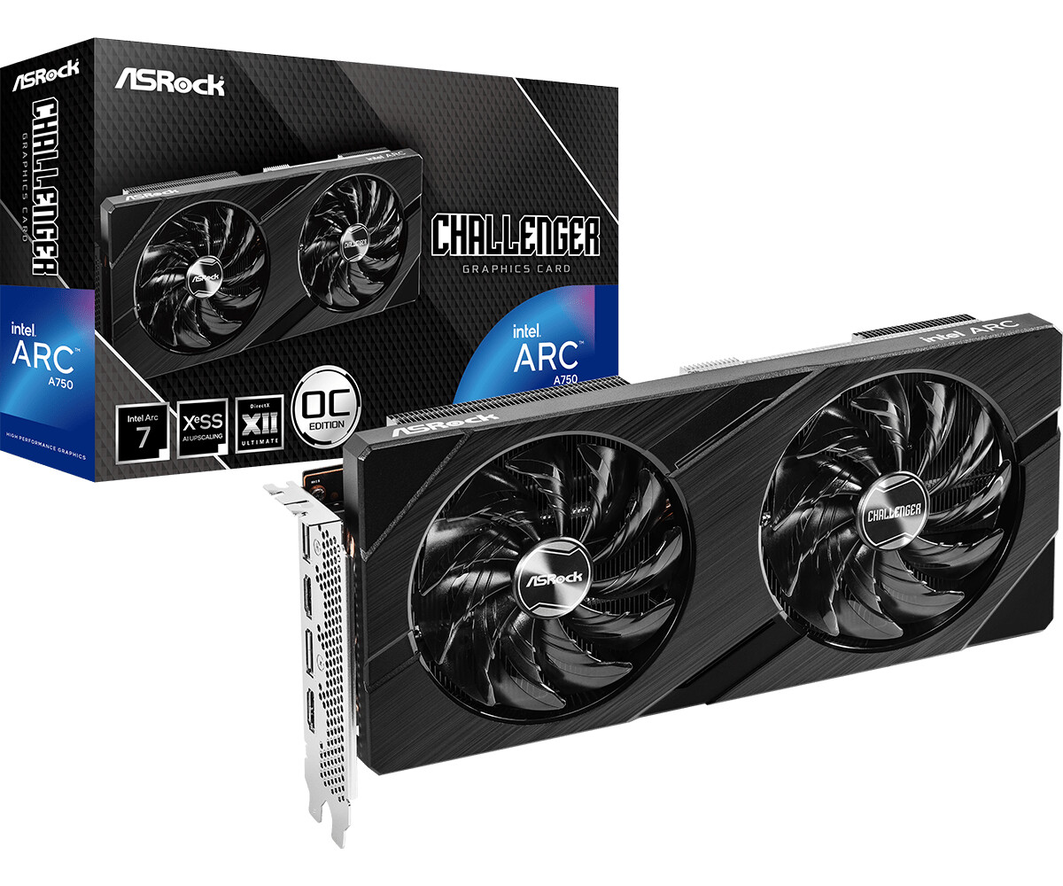
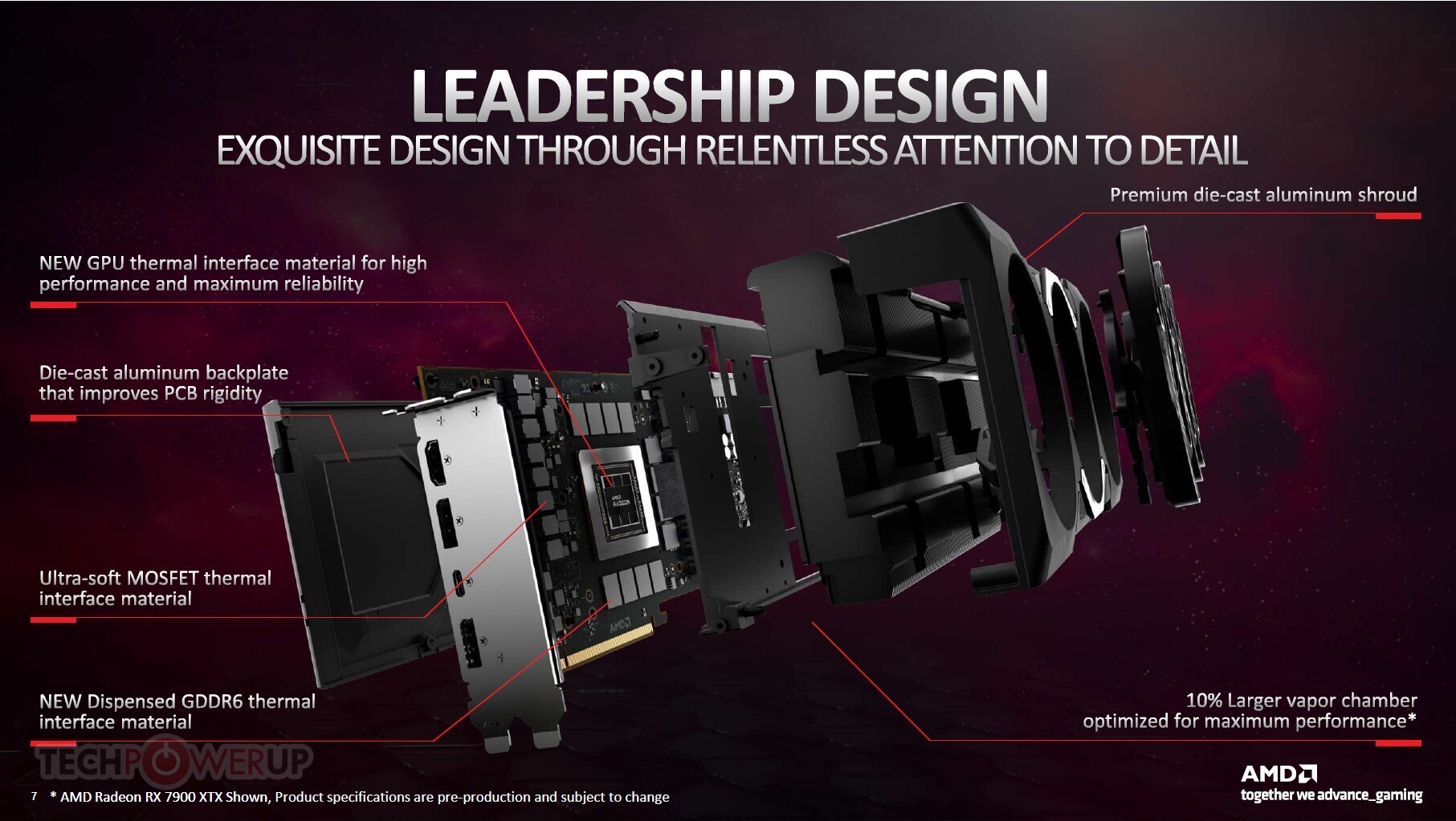
Intel Arc A750 Price Cut—Now Starts at $250

Intel cut the baseline prices of its Arc A750 performance-segment graphics card. The card now starts at USD $249, down from its launch price of $289 for the first-party reference-design card. Among the handful custom-design board partners for the A750 are Acer, Gunnir, and ASRock. The A750 targets maxed-out AAA gaming at 1080p, although the card is capable of higher resolutions with the Intel XeSS performance enhancement.

Based on the 6 nm ACM-G10 silicon, the A750 is endowed with 3,584 unified shaders across 28 Xe Cores or 448 EUs, 224 TMUs, 112 ROPs, and 8 GB of 16 Gbps GDDR6 memory across the chip's full 256-bit wide memory interface (512 GB/s memory bandwidth). The card has a typical board power of 225 W, draws it from a combination of 8-pin and 6-pin PCIe power connectors; and has modern display outputs that include HDMI 2.0 and DisplayPort 2.1. The Arc "Alchemist" family of GPUs meets the full DirectX 12 Ultimate feature-set, including real-time ray tracing. They also have regular driver updates with day-zero optimization for big game releases.
Many Thanks to TumbleGeorge for the tip.

Intel Arc A380 MXM Card Surfaces with 50-75 W Power Limits

A Chinese OEM put a desktop Intel Arc "Alchemist" A380 GPU on an MXM board for notebooks and mobile workstations with upgradable graphics. This isn't the mobile A380M, but rather the desktop A380 that has been designed into an MXM 3.1 type-A board that's capable of PCIe Gen 4 x8. The 6 nm ACM-G11 ASIC is flanked by three GDDR6 memory chips that make the board's 6 GB of memory across its 96-bit memory bus. What's interesting about this board is its tight power limits, which are set at 50 W, that can draw up to 75 W. The card puts out three HDMI and one DP outputs. Its cooling solution mount-hole spacing appears to match that of the popular GeForce GTX 1050 Ti.

GUNNIR Outs 16GB Arc A770 Photon Graphics Card with Triple-Fan Cooler

GUNNIR, the Chinese Intel Arc board partner, unveiled a 16 GB version of its Arc A770 Photon graphics card with specs that partially match Intel's A770 16 GB Limited Edition. Custom-design versions of the A770, such as the one from ASRock Phantom Gaming, only come with 8 GB of memory. The card comes with GUNNIR's heaviest dual-slot, triple-fan cooling solution. While the card offers an overclocked GPU, with the A770 running at 2.40 GHz (compared to 2.10 GHz reference), the memory runs at the same 16 Gbps GDDR6-effective speed as the A770 8 GB version, and not the 17.5 Gbps that the A770 16 GB Limited Edition comes with. This leaves you with a still-respectable 512 GB/s of memory bandwidth on tap. The card draws power from two 8-pin PCIe power connectors. GUNNIR is pricing the card at RMB ¥3,199 ($470).

NVIDIA GeForce RTX 4060 Ti Possible Specs Surface—160 W Power, Debuts AD106 Silicon

NVIDIA's next GeForce RTX 40-series "Ada" graphics card launch is widely expected to be the GeForce RTX 4070 (non-Ti), and as we approach Spring 2023, the company is expected to ramp up to the meat of its new generation, with xx60-segment, beginning with the GeForce RTX 4060 Ti. This new performance-segment SKU debuts the 4 nm "AD106" silicon. A set of leaks by kopite7kimi, a reliable source with NVIDIA leaks, shed light on possible specifications.

The RTX 4060 Ti is based on the AD106 silicon, which is expected to be much smaller than the AD104 powering the RTX 4070 series. The reference board developed at NVIDIA, codenamed PG190, is reportedly tiny, and yet it features the 16-pin ATX 12VHPWR connector. This is probably set for 300 W at its signal pins, and adapters included with graphics cards could convert two 8-pin PCIe into one 300 W 16-pin connector. The RTX 4060 Ti is expected to come with a typical graphics power value of 160 W.

MINISFORUM HX99G 6900HX + RX 6600M Mini PC Goes on Sale

Minisforum introduced a new variant called HX99G in its Neptune portfolio today. It is an upgraded version of the first member, the HX90G (5900HX processor + RX6600M GPU), which was announced in May 2022 before going up for sale in September 2022. The Neptune HX99G looks practically identical to the HX90G. Measuring 205 x 203 x 69 mm (8.1" x 8" x 2.7"), both models feature 45 watts, 8-cores/16-threads graphics and the same laptop-class discrete GPU. However, it updates the Ryzen 9 5900HX with a faster Ryzen 9 6900HX and replaces the two DP ports with two speedier USB4 ports.

R9 6900HX integrates all eight cores based on the Zen 3+ microarchitecture. It's clocked at 3.3 (guaranteed base clock) to 4.9 GHz (max boost). Ryzen 6000 brings a slew of technological advancements, like support for USB 4, PCI-E Gen 4, DDR5-4800MT/s, WIFI 6 and Bluetooth 5.2. The other AMD performance component is the RDNA 2 graphics architecture Radeon RX 6600M (GDDR6 8 GB) with a TDP of up to 100 watts. Users can expect to utilize the full performance of this dedicated GPU to handle professional-class photo and video editing as well as content creation. Also, this GPU packs enough firepower to hit 60 frames per second at 1080p (depending on the specific game and settings).

QoQ Decline in DRAM ASP Will Moderate to Around 13~18% for 1Q23, but Slump Will Continue, Says TrendForce

TrendForce's latest analysis of the DRAM market finds that the inventory pressure on suppliers remain significant due to the persistently weak demand for consumer electronics. Among the top three DRAM suppliers, only Samsung has seen a slight drop in inventory level thanks to its highly competitive pricing strategy. To prevent DRAM prices as a whole from making another sharp dive, a few suppliers such as Micron have been cutting production. Therefore, the QoQ decline in DRAM prices are projected to shrink to around 13~18% for 1Q23. However, the slump will have yet to reach the bottom at that time. Regarding the QoQ changes in the prices of the major categories of DRAM products for 1Q23, PC DRAM and server DRAM are projected to again register a drop that is near 20%. Conversely, mobile DRAM will experience the smallest price decline because its profit margin is ready the thinnest.

AMD Outs Radeon RX 7600M and RX 7600S RDNA3 Mobile Discrete GPUs

AMD today released its first mobile discrete GPUs based on its latest RDNA3 graphics architecture, the Radeon RX 7600M series, and the RX 7600S series. Although based on the latest architecture, AMD decided to built these GPUs on monolithic 6 nm dies, along with many of the power-management features incorporated from Ryzen 6000-series "Rembrandt" processors. The unnamed silicon these GPUs are based on physically features 32 RDNA3 compute units (2,048 stream processors), along with the updated dual instruction-issue rate SIMD components, 2nd generation Ray Accelerators, and AI acceleration. The silicon also features a 128-bit GDDR6 memory interface, supporting speeds of up to 18 Gbps.

The Ryzen 7600M series consists of the top RX 7600M XT with 32 CU, and the slightly lower RX 7600M with 28 CU. Both come with 8 GB of GDDR6 memory across the chip's 128-bit memory interface. The RX 7600M XT uses 18 Gbps memory clocks, while the RX 7600M uses 16 Gbps. The RX 7600M XT has a power band of 75 W to 120 W, while the RX 7600M needs 50 W to 90 W. The RX 7700S and RX 7600S have the same core-configurations as the RX 7600M XT and RX 7600M, respectively, but lower power draw (up to 100 W for the RX 7700S, and up to 75 W for the RX 7600S). Both GPUs feature updated display- and media-acceleration engines, with support for QHD+ displays up to 240 Hz. AMD claims that the RX 7600M XT beats the performance of desktop NVIDIA GeForce RTX 3060 12 GB.

SK hynix to Showcase Energy-Efficient, High-Performance Memory Products at CES 2023

SK hynix Inc. announced today that it will showcase a number of its core and brand-new products at the CES 2023, the most influential tech event in the world taking place in Las Vegas from Jan. 5th through Jan. 8th. The products, introduced under the theme of the "Green Digital Solution," as part of the SK Group's "Carbon-Free Future" campaign, are expected to attract Big Tech customers and experts given the significant improvement in performance and energy efficiency compared with the previous generation as well as the effect of lessening the impact on the environment.

Attention on energy-efficient memory chips has been on the rise as global tech companies pursue products that process data faster, while consuming less energy. SK hynix is confident that its products to be displayed at the CES 2023 will meet customers' such needs with outstanding performance per watt and performance. The core product put forward at the show is PS1010 E3.S, an eSSD product composed of multiple 176-layer 4D NAND that supports the fifth generation of the PCIe interface.

Achronix Announces Speedster7t AC7t1500 FPGA General Availability

In a continuing commitment to enabling industry-leading data acceleration in heterogeneous compute environments, Achronix Semiconductor Corporation, the industry's only independent supplier of high-end FPGAs and eFPGA IP solutions, today announced the production release of its AC7t1500 FPGA and the addition of the power-efficient AC7t800 FPGA to the Achronix Tool Suite.

"The Speedster 7t product family offers unprecedented FPGA-based performance for data acceleration applications," said Steve Mensor, VP of Marketing and Business Development at Achronix. "The release of the AC7t1500 to production along with the addition of the AC7t800 in our ACE design tools gives customers multiple options from this industry-leading, high-performance family that offers FPGA programmability with ASIC-level performance. These advancements give customers confidence that they can design on a robust, validated FPGA product family that meets their high-performance and high-bandwidth needs."

Sapphire Also Announces the Pulse Radeon RX 7900-series Graphics Cards

SAPPHIRE Technology also launches the SAPPHIRE PULSE AMD Radeon RX 7900 Series Graphics Cards for great gaming performance at excellent value. The PULSE AMD Radeon RX 7900 XTX Graphics Card headlines with 96 Compute units and 6144 stream processors running with a Boost Clock of up to 2525 MHz and a Game Clock of up to 2330 MHz. The PULSE AMD Radeon RX 7900 XT features 84 Compute Units with 5376 stream processors, a Boost Clock of up to 2450 MHz and a Game Clock of up to 2075 MHz. Visualize the latest 24 GB and 20 GB respectively of GDDR6 high-speed memory clocked at 20 Gbps Effective with 96 MB and 80 MB respectively of Infinity Cache. The graphics card supports up to 4 output ports including 2x HDMI 2.1 and 2x DisplayPort 2.1 ports with DSC outputs to align with the latest monitors on the market.

The SAPPHIRE PULSE AMD Radeon RX 7900 Series Graphics Cards run on SAPPHIRE's distinguished Tri-X Cooling Technology which work in tandem with the Intelligent Fan Control and Precision Fan Control features to keep temperatures low and fan noise low. Stability and reliability are key pillars of the PULSE AMD Radeon RX 7900 Series Graphics Cards. The High TG Copper PCB design enables stable and reliable performance resulting in a low temperature and low noise PCB component. The crucial Fuse Protection feature is built into the circuit of the external PCIe power connector to keep the components safe. As part of SAPPHIRE's motto of long-lasting components, Dual-Ball Bearing Fans are fitted to increase the lifespan of the Graphics Cards.

Sapphire Announces the Nitro+ Radeon RX 7900-series GPUs with Vapor-X Cooling

SAPPHIRE Technology announces the heavily anticipated NITRO+ AMD Radeon RX 7900 Vapor-X Series Graphics Cards, with breakthrough performance and incredible clock speeds for both gamers and creators 4K and beyond. The cards are crafted with SAPPHIRE's signature cutting-edge cooling features, quality of life components and engineered to push high framerates with the optimal balance of heat and noise.

At the core of the NITRO+ Graphics Cards series are the technologies of the SAPPHIRE PANTHEON Suite of permanent features. SAPPHIRE PANTHEON guarantees supreme cooling technology and other distinct features exclusive to NITRO+ graphics cards. Each NITRO+ iconic feature stands as strong and permanent as the pillars of the PANTHEON. Every NITRO+ Graphics Card guarantees the presence of the stable, reliable and innovative SAPPHIRE PANTHEON suite of features.

PNY GeForce RTX 4070 Ti Specifications Leak, Similar to the Canceled RTX 4080 12 GB Edition

VideoCardz has obtained images and specifications of PNY's two upcoming GeForce RTX 4070 Ti models. According to the latest leak, these GPUs are equipped with 7680 CUDA cores and 12 GB of GDDR6X memory. This configuration resembles the canceled GeForce RTX 4080 12 GB edition card, which confirms that NVIDIA will rebrand it under the RTX 4070 Ti naming scheme. PNY has prepared GeForce RTX 4070 Ti XLR8 VERTO and VERTO GPUs, with the difference in cooler design and applied factory overclocking. The XLR8 version bears the same cooler as the RTX 4080 XRL8 card, adapted for the RTX 4070 Ti GPU SKU. This design should naturally offer greater overclocking performance than the regular VERTO SKU.

The render below looks like the 16-pin 12VHPWR power connector remains on these cards and that PNY has not swapped it for another solution. We expect to hear more about these cards on January 5th, when NVIDIA plans to launch.

NVIDIA GeForce RTX 4060 Ti to Feature Shorter PCB, 220 Watt TDP, and 16-Pin 12VHPWR Power Connector

While NVIDIA has launched high-end GeForce RTX 4090 and RTX 4080 GPUs from its Ada Lovelace family, middle and lower-end products are brewing to satisfy the entire consumer market. Today, according to the kopite7kimi, a well-known leaker, we have potential information about the configuration of the upcoming GeForce RTX 4060 Ti graphics card. Featuring 4352 FP32 CUDA cores, the GPU is powered by an AD106-350-A1 die. On the die, there is 32 MB of L2 cache. To pair, it has 8 GB of GDDR6 18 Gbps memory, which should be enough to power games at 1440p resolution, which this card is aiming for.

The design of the cards reference PG190 PCB is supposedly very short, making it ideal for ITX-sized designs we could see from NVIDIA's AIB partners. Interestingly, with a TDP of 220 Watts, the reference card is powered by the infamous 16-pin 12VHPWR connector, capable of supplying 600 Watts of power. This choice of connector is unclear; however, it could be NVIDIA's push to standardize its usage across all products in the Ada Lovelace family stack. While the card should not need the full potential of the connector, it signals that the company could only be using this type of connector for all of its future designs.

ASRock Launches AMD Radeon RX 7900 Series Graphics Cards Unlock Your Gaming Power and Creativity

ASRock, the leading global motherboard, graphics card and mini PC manufacturer, today launched the new AQUA, Taichi and Phantom Gaming series graphics cards based on AMD Radeon RX 7900 Series GPUs.

The new graphics cards are built on the groundbreaking AMD RDNA 3 architecture with chiplet technology. AMD RDNA 3 architecture delivers up to 54% more performance per watt than AMD RDNA 2, features the world's fastest interconnect linking the graphics and memory system chiplets at up to 5.3 TB/s, and offers up to 96 new unified compute units and second-generation AMD Infinity Cache technology. It also delivers increased AI throughput that provides up to 2.7X higher AI performance, and rearchitected compute units with second-generation ray tracing technology that provides up to 1.8X higher ray tracing architectural performance in select titles versus AMD RDNA 2 architecture.

NVIDIA Gives RTX A6000 "Ada" Professional Graphics a Quiet Launch, Starting $7377

NVIDIA is ready to launch its RTX A6000 series "Ada" professional-visualization graphics cards. These cards are targeted at the same market demographic as the NVIDIA Quadro series of the old—serious 3D content creation. The RTX A6000 leads the pack, and is based on the 4 nm "AD102" silicon (the same one powering the GeForce RTX 4090). The A6000 is better endowed than the RTX 4090 at the silicon-level, although operating at lower GPU clock-speeds, for its tighter 300 W power-limit (compared to 450 W of the RTX 4090).

The A6000 "Ada" is endowed with 18,176 CUDA cores across 142 SM, compared to the 16,384 CUDA cores across 128 SM of the RTX 4090. It also gets a higher number of Tensor cores, at 568. The defining differentiator between the A6000 and RTX 4090 has to be memory, with the pro-vis card getting 48 GB of ECC GDDR6 memory across the chip's 384-bit memory bus, clocked at 20 Gbps (960 GB/s memory bandwidth); compared to the 24 GB of 21 Gbps GDDR6X (1008 GB/s) of the RTX 4090. Also, the card enables all three NVDEC and NVENC video hardware-accelerators physically present on the AD102, for six independent accelerated transcoding streams.

AMD RDNA3 Second-largest Navi 32 and Third-largest Navi 33 Shader Counts Leaked

The unified shader (stream processor) counts of AMD's upcoming second- and third-largest GPUs based on the RDNA3 graphics architecture, have been leaked in some ROCm code, discovered by Kepler_L2 on Twitter. The "performance.hpp" file references "Navi 32" with a compute unit count of 60, and the "Navi 33" with 32 compute units. We know from the "Navi 31" specifications that an RDNA3 compute unit still amounts to 64 stream processors (although with significant IPC uplifts over the RDNA2 stream processor due to dual-instruction issue-rate).

60 compute units would give the "Navi 32" silicon a stream processor count of 3,840, a 50% numerical increase over the 2,560 of its predecessor, the "Navi 22," powering graphics cards such as the Radeon RX 6750 XT. Meanwhile, the 32 CU count of the "Navi 33" amounts to 2,048 stream processors, which is numerically unchanged from that of the "Navi 23" powering the RX 6650 XT. The new RDNA3 compute unit has significant changes over RDNA2, besides the dual-issue stream processors—it gets second-generation Ray Accelerators, and two AI accelerators for matrix-multiplication.

Samsung Develops GDDR6W Memory Standard: Double the Bandwidth and Density of GDDR6 Through Packaging Innovations

As advanced graphics and display technologies develop, they are blurring the lines between metaverse and our everyday experience. Much of this important shift is being made possible by the advancement of memory solutions designed for graphics products. One of the biggest challenges for improving virtual reality is taking the complexities of real-world objects and environments and recreating them in a virtual space. Doing so requires massive memory and increased computing power. At the same time, the benefits of creating more true-to-life metaverse will be far reaching, including real-life simulations of complicated scenarios and more, sparking innovation across a number of industries.

This is the central idea behind one of the most popular concepts in virtual reality: digital twin. A digital twin is a virtual representation of an object or space. Updated in real-time in accordance with the actual environment, a digital twin spans the lifecycle of its source and uses simulation, machine learning and reasoning to help decision-making. While until recently this was not feasible proposition due to limitations on data processing and transference, digital twins are now gaining traction thanks to availability of high bandwidth technologies.

AMD Confirms Radeon RX 7900 Series Clocks, Direct Competition with RTX 4080

AMD in its technical presentation confirmed the reference clock speeds of the Radeon RX 7900 XTX and RX 7900 XT RDNA3 graphics cards. The company also made its first reference to a GeForce RTX 40-series "Ada" product, the RTX 4080 (16 GB), which is going to launch later today. The RX 7900 XTX maxes out the "Navi 31" silicon, featuring all 96 RDNA3 compute units or 6,144 stream processors; while the RX 7900 XT is configured with 84 compute units, or 5,376 stream processors. The two cards also differ with memory configuration. While the RX 7900 XTX gets 24 GB of 20 Gbps GDDR6 across a 384-bit memory interface (960 GB/s); the RX 7900 XT gets 20 GB of 20 Gbps GDDR6 across 320-bit (800 GB/s).

The RX 7900 XTX comes with a Game Clocks frequency of 2300 MHz, and 2500 MHz boost clocks, whereas the RX 7900 XT comes with 2000 MHz Game Clocks, and 2400 MHz boost clocks. The Game Clocks frequency is more relevant between the two. AMD achieves 20 GB memory on the RX 7900 XT by using ten 16 Gbit GDDR6 memory chips across a 320-bit wide memory bus created by disabling one of the six 64-bit MCDs, which also subtracts 16 MB from the GPU's 96 MB Infinity Cache memory, leaving the RX 7900 XT with 80 MB of it. The slide describing the specs of the two cards compares them to the GeForce RTX 4080, which is what the two could compete more against, especially given their pricing. The RX 7900 XTX is 16% cheaper than the RTX 4080, and the RX 7900 XT is 25% cheaper.

AMD Radeon RX 7900 XTX Reference Design PCB and Cooler Detailed

AMD Radeon RX 7900 XTX reference-design isn't a first-party product with limited availability like the NVIDIA Founders Edition; but rather a classic reference-design that's sold by AMD's add-in board partners under their marquee (without sticking their own labels on the product). AMD and its partners internally refer to reference-design cards as "MBA cards" (made by AMD cards). The company gave us a technical overview of the reference-design PCB. As with every reference AMD PCB for the past several generations, the RX 7900 XTX PCB has a premium selection of components. The card uses an expensive 14-layer PCB with 4 additional layers of 2-oz copper. 14-layer PCBs are typically used with enterprise-grade products, and graphics cards typically tend to have PCB layer counts of around 10. The PCB also uses ITEQ IT-170GRA epoxy and laminate materials, which enable a glass transition temperature (Tg) of 175 °C (no, the GPU won't get anywhere near as hot).

The reference-design RX 7900 XTX PCB draws power from two 8-pin PCIe power connectors. With the typical board power of the RX 7900 XTX rated at 355 W, this falls inside the 375 total power-draw capability when you add up the 150 W input from the two connectors, and 75 W from the PCIe slot. AMD worked to minimize power-draw spikes at least from the PCIe slot. Excursions, if any, should be localized to the 8-pin power connectors. The card features 20-phase VRM solution, using "high efficiency" DrMOS power-stage phases (could be very high current). The "Navi 31" GPU is surrounded by 12 GDDR6 memory chips given the GPU's 384-bit memory interface. Two of these memory pads could end up unused on the RX 7900 XT, which has a 320-bit memory interface. Display outputs of the RX 7900 series include two standard-size DisplayPort 2.1, one USB type-C with DisplayPort passthrough; and one HDMI 2.1a.

AMD Explains the Economics Behind Chiplets for GPUs

AMD, in its technical presentation for the new Radeon RX 7900 series "Navi 31" GPU, gave us an elaborate explanation on why it had to take the chiplets route for high-end GPUs, devices that are far more complex than CPUs. The company also enlightened us on what sets chiplet-based packages apart from classic multi-chip modules (MCMs). An MCM is a package that consists of multiple independent devices sharing a fiberglass substrate.

An example of an MCM would be a mobile Intel Core processor, in which the CPU die and the PCH die share a substrate. Here, the CPU and the PCH are independent pieces of silicon that can otherwise exist on their own packages (as they do on the desktop platform), but have been paired together on a single substrate to minimize PCB footprint, which is precious on a mobile platform. A chiplet-based device is one where a substrate is made up of multiple dies that cannot otherwise independently exist on their own packages without an impact on inter-die bandwidth or latency. They are essentially what should have been components on a monolithic die, but disintegrated into separate dies built on different semiconductor foundry nodes, with a purely cost-driven motive.

AMD RDNA3 Navi 31 GPU Block Diagram Leaked, Confirmed to be PCIe Gen 4

An alleged leaked company slide details AMD's upcoming 5 nm "Navi 31" GPU powering the next-generation Radeon RX 7900 XTX and RX 7900 XT graphics cards. The slide details the "Navi 31" MCM, with its central graphics compute die (GCD) chiplet that's built on the 5 nm EUV silicon fabrication process, surrounded by six memory cache dies (MCDs), each built on the 6 nm process. The GCD interfaces with the system over a PCI-Express 4.0 x16 host interface. It features the latest-generation multimedia engine with dual-stream encoders; and the new Radiance display engine with DisplayPort 2.1 and HDMI 2.1a support. Custom interconnects tie it with the six MCDs.

Each MCD has 16 MB of Infinity Cache (L3 cache); and a 64-bit GDDR6 memory interface (two 32-bit GDDR6 paths). Six of these add up to the GPU's 384-bit GDDR6 memory interface. In the scheme of things, the GPU has a contiguous and monolithic 384-bit wide memory bus, because every modern GPU uses multiple on-die memory controllers to achieve a wide memory bus. "Navi 31" hence has a total Infinity Cache size of 96 MB—which may be less in comparison to the 128 MB on "Navi 21," but AMD has shored up cache sizes across the GPU. The L0 caches on the compute units is now increased numerically by 240%. The L1 caches by 300%, and the L2 cache shared among the shader engines, by 50%. The RX 7900 XTX is confirmed to use 20 Gbps GDDR6 memory in this slide, for 960 GB/s of memory bandwidth.

AMD Navi 31 RDNA3 GPU Pictured

Here's the first picture of the "Navi 31" GPU at the heart of AMD's fastest next-generation graphics cards. Based on the RDNA3 graphics architecture, this will mark an ambitious attempt by AMD to build the first multi-chip module (MCM) client GPU featuring more than one logic die. MCM GPUs aren't new in the enterprise space with Intel's "Ponte Vecchio," but this would be the first such GPU meant for hardcore gaming graphics products. AMD had made MCM GPUs in the past, but those have been packages with just one logic die, surrounded by memory stacks. "Navi 31" is an MCM of as many as eight logic dies, and no memory stacks (no, those aren't HBM stacks in the picture below).

It's rumored that "Navi 31" features one or two SIMD chiplets dubbed GCDs, featuring the GPU's main number crunching machinery, the RDNA3 compute units. These chiplets are likely built on the most advanced silicon fabrication node, likely TSMC 5 nm EUV, but we'll see. The GDDR6 memory controllers handling the chip's 384-bit wide GDDR6 memory interface, will be located on separate chiplets built on a slightly older node, such as TSMC 6 nm. This is not multi-GPU-a-stick, because both SIMD chiplets have uniform access to the entire 384-bit wide memory bus (which is not 2x 192-bit but 1x 384-bit), besides the other ancillaries. The "Navi 31" MCM are expected to be surrounded by JEDEC-standard 20 Gbps GDDR6 memory chips.

AMD Radeon RX 7000 RDNA3 To Launch Early December

AMD's next-generation Radeon RX 7000-series graphics cards based on the RDNA3 graphics architecture, are expected to launch in early-December 2022, according to greymon55, a reliable source with AMD leaks. The cards will be unveiled at a media event to be held on November 3, 2022, with market availability following a month after (between 1st to 5th December). The company is expected to take a top-down product-stack release cycle similar to that of NVIDIA, with the release of two of its top SKUs, the Radeon RX 7900 XTX and the RX 7900 XT. Both these cards are based on the 5 nm Navi 31 MCM GPU. This will be AMD's first client-graphics MCM GPU with more than one logic die. The company has a decade of experience with MCMs, but past generations have been one logic die surrounded with on-package HBM. Navi 31 has on-package logic chiplets, but discrete GDDR6 memory, like most other GPUs in the market today. It's rumored that the company is targeting a 100% performance uplift over the previous-generation, which means team-red is on the prowl to compete with NVIDIA's fastest SKUs, including the RTX 4090 and upcoming RTX 4080.

NVIDIA Partners Quietly Launch GeForce RTX 3060 with 8GB (128-bit) Memory

NVIDIA's add-in board partners today began quietly launching the GeForce RTX 3060 8 GB, a variant of the RTX 3060 with a third of its memory size and memory bus-width sawed off. The RTX 3060, NVIDIA's best-selling desktop graphics SKU from the RTX 30-series "Ampere," originally launched with 12 GB of GDDR6 memory across a 192-bit wide memory bus, which at its reference speed of 15 Gbps (GDDR6-effective), makes 360 GB/s of memory bandwidth. The new variant comes with 8 GB of GDDR6 memory across a narrower 128-bit memory interface, with the same 15 Gbps data-rate, which works out to 240 GB/s memory bandwidth.

Besides memory size, bus-width, and bandwidth; NVIDIA hasn't tinkered with the core-configuration with the RTX 3060 8 GB. It still comes with 3,584 CUDA cores across 28 SM, which work out to 112 Tensor cores, 28 RT cores, 112 TMUs, and 48 ROPs. The GPU's base frequency is set at 1320 MHz, and boost frequency at 1777 MHz—same as the original RTX 3060. Even the typical graphics power is unchanged, at 170 W. The new 8 GB variant doesn't replace the original, but is being positioned a notch below it, possibly to compete against the likes of the Radeon RX 6600 (non-XT), and perhaps even the Arc A750.

AMD Radeon RX 7900 XTX to Lead the RDNA3 Pack?

AMD is reportedly bringing back the "XTX" brand extension to the main marketing names of its upcoming Radeon RX 7000-series SKUs. The company had, until now, reserved the "XTX" moniker for internal use, to denote SKUs that max out all hardware available on a given silicon. The RX 7000-series introduce the company's next-generation RDNA3 graphics architecture, and will see the company introduce its chiplets packaging design to the client-graphics space. The next-generation "Navi 31" GPU will likely be the first of its kind: while multi-chip module (MCM) GPUs aren't new, this would be the first time that multiple logic chips would sit on a single package for client GPUs. AMD has plenty of experience with MCM GPUs, but those have been single logic chips surrounded by memory stacks. "Navi 31" uses multiple logic chips on a package; which is then wired to conventional discrete GDDR6 memory devices like any other client GPU.

The rumored Radeon RX 7900 XTX is features 12,288 stream processors, likely across two logic tiles that contain the SIMD components. These tiles are [for now] rumored to be built on the TSMC N5 (5 nm EUV) foundry process. The Display CoreNext (DCN), and Video CoreNext (VCN) components, as well as the GDDR6 memory controllers, will be built on separate chiplets that are likely built on TSMC N6 (6 nm). The "Navi 31" has a 384-bit wide memory interface. This is 384-bit and not "2x 192-bit," because the logic tiles don't have memory interfaces of their own, but rely on memory controller tiles shared between the two logic tiles, much in the same as a dual-channel DDR4 memory interface being shared between the two 8-core CPU chiplets on a Ryzen 5950X processor.
Return to Keyword Browsing
Jul 5th, 2025 17:50 CDT change timezone

New Forum Posts

Popular Reviews

TPU on YouTube

Controversial News Posts