News Posts matching #GP102

Return to Keyword Browsing

NVIDIA P102-100 Cryptomining Graphic Card Surfaces

The truth of the matter is that the cryptocurrency boom isn't losing strength yet, and graphics card manufacturers are more than happy to profit off this phenomenon. However, one must have the right tools to mine cryptocurrency effectively. NVIDIA is keen to provide cryptominers with the necessary hardware as they ready their latest GP102-100 card for launch. The GP102-100 should sound familiar to most enthusiasts since it employs the same GP102 chip used in the mainstream GeForce GTX 1080 Ti and GTX Titan Xp graphics cards. Nevertheless, NVIDIA made a few modifications in order to maintain the hash rate while lowering the price at the same time. In other words, we're basically dealing with a gimped version of the GP102 chip with less memory channels, shader cores, and memory.

The Inno3D P102-100 is the first model to show up in the wild. The card packs 3,200 CUDA cores clocked at 1582 MHz and 5 GB of GDDR5X memory operating at 10 Gbps across a 320-bit wide memory interface. Inno3D is utilizing their Twin X2 cooling solution to cool the card. This solution features five heatpipes to draw the heat away from the GPU and two fans to provide active cooling. Being a mining-oriented model, the Inno3D P102-100 lacks a bracket and display outputs. It also only requires four PCIe lanes to function. The Inno3D P102-100 has a 250W TDP rating and draws power from a pair of 8-pin PCIe power connectors. According to Inno3D, their card is capable of mining Ethereum with a hash rate of 47 MH/s which easily beats a GeForce GTX 1080 Ti and GTX Titan Xp. Pricing is unknown at the writing of this article.

EVGA Intros GeForce GTX 1080 Ti K|NGP|N Hydro Copper

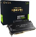
EVGA today introduced its flagship graphics card, the GeForce GTX 1080 Ti K|ngp|n Hydro Copper (model: 11G-P4-6799), tuned by the legendary overclocker Vince "K|ngp|n" Lucido himself. The card features the choicest VRM components, binned "GP102" ASIC and GDDR5X memory chips, to support not just the highest overclocking headroom among EVGA's lineup, but also its highest factory-overclocked speeds of 1582 MHz core, 1695 MHz GPU Boost, and 11.00 GHz (GDDR5X-effective) memory clocks.

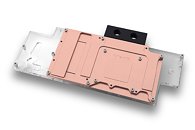
The card is intended to be plumbed to your own liquid-cooling loop, and comes with an all-copper, full-coverage water-block. You also get EVGA's iCX technology, which puts 9 thermal sensors across various points in the card. Available now (in limited stocks), exclusively through EVGA's own online store, the card is priced at USD $1,249.

NVIDIA Announces the TITAN Xp Star Wars Collectable Editions

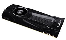
NVIDIA has announced two new collector's edition NVIDIA TITAN Xp GPUs created for the ultimate Star Wars fan. The new Jedi Order and Galactic Empire editions of the NVIDIA TITAN Xp have been crafted to reflect the look and feel of the Star Wars galaxy.
These new Star Wars collector's edition GPUs pay homage to the light side/dark side dichotomy, and contain hints of the Star Wars galaxy, such as the hilt of Luke Skywalker's lightsaber and light panels reminiscent of the Death Star.

The Jedi Order GPU simulates the wear and tear and battle-worn finish of many items used by the Rebel Alliance, resulting from its diecast aluminum cover being subjected to an extensive, corrosive salt spray. Conversely, the Galactic Empire GPU's finish features simple, clean lines, emulating the high-end, orderly nature of the resource-rich Empire. Both versions have multiple windowed areas to showcase internals and lighting, evoking each faction's lightsabers, green and red, respectively. The finishes of both versions took over a year to perfect.

NVIDIA Unlocks Certain Professional Features for TITAN Xp Through Driver Update

In a bid to preempt sales of the Radeon Pro Vega Frontier Edition, and the Pro WX 9100, NVIDIA expanded the feature-set of its consumer-segment TITAN Xp graphics card, with certain features reserved for its Quadro family of graphics cards, through a driver update. NVIDIA is rolling out its latest GeForce software update, which adds professional features for applications such as Maya, unlocking "3X more performance" for the software.

Priced at USD $1,199, the TITAN Xp packs a full-featured "GP102" graphics processor, with 3,840 CUDA cores, 240 TMUs, 96 ROPs, and 12 GB of GDDR5X memory across the chip's 384-bit wide memory interface. At its given memory clock of 11.4 GHz (GDDR5X-effective), the card has a memory bandwidth of 547.6 GB/s, which is higher than the 484 GB/s of the Radeon Pro Vega Frontier Edition.

DOWNLOAD: NVIDIA GeForce 385.12 for TITAN Xp

NVIDIA "Pascal" Based Mining GPU Lineup Detailed

GPU-accelerated crypto-currency mining poses a threat to the consumer graphics industry, yet the revenues it brings to GPU manufacturers are hard to turn away. The more graphics cards are bought up by crypto-currency miners, the fewer there are left for gamers and the actual target-audience of graphics cards. This is particularly bad for AMD, as fewer gamers have Radeon graphics cards as opposed to miners; which means game developers no longer see AMD GPU market-share as an amorphous trigger to allocate developer resources in optimizing their games to AMD architectures.

To combat this, both AMD and NVIDIA are innovating graphics cards designed specifically for crypto-currency mining. These cards are built to a cost, lack display outputs, and have electrical and cooling mechanisms designed for 24/7 operation, even if not living up to the durability standards of real enterprise-segment graphics cards, such as Radeon Pro series or Quadro. NVIDIA's "Pascal" GPU architecture is inherently weaker than AMD's "Polaris" and older Graphics CoreNext architectures at Ethereum mining, owing in part to Pascal's lack of industry-standard asynchronous compute. This didn't deter NVIDIA from innovating a lineup of crypto-mining SKUs based on its existing "Pascal" GPUs. These include the NVIDIA P104 series based on the "GP104" silicon (on which the GTX 1080 and GTX 1070 are based); and P106 series based on the "GP106" silicon (GTX 1060 series is based on this chip). NVIDIA didn't tap into its larger "GP102" or smaller "GP107" chips, yet.

Alphacool Eisblock Full-coverage VGA Block for GP102 Boards Pictured

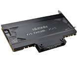
Alphacool rolled the Eisblock GPX-N full-coverage water-block for GeForce GTX 1080 Ti Founders Edition, TITAN X Pascal, and TITAN Xp (they share the same reference PCB). The block features a nickel-plated copper primary material, with an acrylic top, and a metal outer shroud that gives the block an industrial look. Also included is an aluminium back-plate. The block features standard G1/4" fittings.

NVIDIA Announces the TITAN Xp - Faster Than GTX 1080 Ti

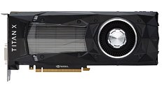
NVIDIA GeForce GTX 1080 Ti cannibalized the TITAN X Pascal, and the company needed something faster to sell at USD $1,200. Without making much noise about it, the company launched the new TITAN Xp, and with it, discontinued the TITAN X Pascal. The new TITAN Xp features all 3,840 CUDA cores physically present on the "GP102" silicon, all 240 TMUs, all 96 ROPs, and 12 GB of faster 11.4 Gbps GDDR5X memory over the chip's full 384-bit wide memory interface.

Compare these to the 3,584 CUDA cores, 224 TMUs, 96 ROPs, and 10 Gbps GDDR5X memory of the TITAN X Pascal, and 3,584 CUDA cores, 224 TMUs, 88 ROPs, and 11 GB of 11 Gbps GDDR5X memory across a 352-bit memory bus, of the GTX 1080 Ti. The GPU Boost frequency is 1582 MHz. Here's the catch - the new TITAN Xp will be sold exclusively through GeForce.com, which means it will be available in very select markets where NVIDIA's online store has a presence.

On NVIDIA's Tile-Based Rendering

Looking back on NVIDIA's GDC presentation, perhaps one of the most interesting aspects approached was the implementation of tile-based rendering on NVIDIA's post-Maxwell architectures. This has been an adaptation of typically mobile approaches to graphics rendering which keeps their specific needs for power efficiency in mind - and if you'll "member", "Maxwell" was NVIDIA's first graphics architecture publicly touted for its "mobile first" design.

This approach essentially divides the screen into tiles, and then rasterizes the entire frame in a per-tile basis. 16×16 and 32×32 pixels are the usual tile sizes, but both Maxwell and Pascal can dynamically assess the required tile size for each frame, changing it on-the-fly as needed and according to the complexity of the scene. This looks to ensure that the processed data has a much smaller footprint than that of the full image rendering - small enough that it makes it possible for NVIDIA to keep the data in a much smaller amount of memory (essentially, the L2 memory), dynamically filling and flushing the available cache as possible until the full frame has been rendered. This means that the GPU doesn't have to access larger, slower memory pools as much, which primarily reduces the load on the VRAM subsystem (increasing available VRAM for other tasks), whilst simultaneously accelerating rendering speed. At the same time, a tile-based approach also lends itself pretty well to the nature of GPUs - these are easily parallelized operations, with the GPU being able to tackle many independent tiles simultaneously, depending on the available resources.

NVIDIA Announces the GeForce GTX 1080 Ti Graphics Card at $699

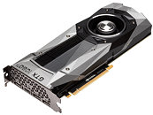
NVIDIA today unveiled the GeForce GTX 1080 Ti graphics card, its fastest consumer graphics card based on the "Pascal" GPU architecture, and which is positioned to be more affordable than the flagship TITAN X Pascal, at USD $699, with market availability from the first week of March, 2017. Based on the same "GP102" silicon as the TITAN X Pascal, the GTX 1080 Ti is slightly cut-down. While it features the same 3,584 CUDA cores as the TITAN X Pascal, the memory amount is now lower, at 11 GB, over a slightly narrower 352-bit wide GDDR5X memory interface. This translates to 11 memory chips on the card. On the bright side, NVIDIA is using newer memory chips than the one it deployed on the TITAN X Pascal, which run at 11 GHz (GDDR5X-effective), so the memory bandwidth is 484 GB/s.

Besides the narrower 352-bit memory bus, the ROP count is lowered to 88 (from 96 on the TITAN X Pascal), while the TMU count is unchanged from 224. The GPU core is clocked at a boost frequency of up to 1.60 GHz, with the ability to overclock beyond the 2.00 GHz mark. It gets better: the GTX 1080 Ti features certain memory advancements not found on other "Pascal" based graphics cards: a newer memory chip and optimized memory interface, that's running at 11 Gbps. NVIDIA's Tiled Rendering Technology has also been finally announced publicly; a feature NVIDIA has been hiding from its consumers since the GeForce "Maxwell" architecture, it is one of the secret sauces that enable NVIDIA's lead.

AMD Radeon Vega Power Connectors Pictured

At its first reveal of the Radeon Vega graphics card on the sidelines of the 2017 International CES show, AMD was careful to conceal the power-connectors of its graphics card prototype (using tissue paper), even though teaser images of the card were splattered all over the web. From this week's reveal of a Radeon Vega graphics card running on an AMD Ryzen 7-1800X powered machine, the veil is off the power connector layout. Apparently, AMD's reference design Radeon Vega 10 graphics card is air-cooled, and it draws power from a combination of 8-pin and 6-pin PCIe power connectors.

NVIDIA's GeForce GTX 1080 (reference) makes do with a single 8-pin connector, although most custom-design GTX 1080 cards feature 6-pin + 8-pin layouts. The GP102-powered TITAN X Pascal reference, too, draws power from 6+8 pin connectors. It's interesting to note here, that the power connectors feature a string of LEDs near their contact points on the PCB. The Radeon R9 Fury X, too has something like this, although the LEDs are used to alert users of faulty power input, or power draw. In the image below, we see that LEDs over only one connector are lit up. Could this indicate that AMD is making sure users are aware that the card isn't drawing power from both connectors all the time?

NVIDIA to Steal AMD's Ryzen Limelight on Feb 28

NVIDIA could attempt to steal the limelight from AMD's 2017 "Capsaicin & Cream" launch event for its Ryzen desktop processors, slated for February 28, with a parallel GeForce GTX event along the sidelines of the 2017 Game Developers' Conference (GDC). At this event, the company is expected to launch its next enthusiast-segment graphics card, the GeForce GTX 1080 Ti. This could at least be a paper-launch, with market availability following through in March.

While the GTX 1080 Ti is a graphics card, and Ryzen a processor (they don't compete), NVIDIA's choice of launch-date could certainly steal some attention away from AMD's big day. Besides launching Ryzen, it wouldn't surprise us if AMD teases its upcoming Radeon "Vega" graphics cards a little more. The GeForce GTX 1080 Ti is expected to be based on the same "GP102" silicon as the company's flagship TITAN X Pascal graphics card, and could be positioned very close to the USD $1,000 mark, given that NVIDIA priced the TITAN X Pascal at a wallet-scorching $1,199.

NVIDIA GeForce GTX 1080 Ti Features 10GB Memory?

Air-cargo shipping manifest descriptions point to the possibility that NVIDIA's upcoming high-end graphics card based on the GP102 silicon, the GeForce GTX 1080 Ti, could feature 10 GB of memory, and not the previously thought of 12 GB, which would be the same amount as the TITAN X Pascal. NVIDIA apparently is getting 10 GB to work over a 384-bit wide memory interface, likely using chips of different densities. The GTX 1080 Ti is also rumored to feature 3,328 CUDA cores, 208 TMUs, and 96 ROPs.

NVIDIA has, in the past, used memory chips of different densities to achieve its desired memory amount targets over limited memory bus widths. The company achieved 2 GB of memory across a 192-bit wide GDDR5 memory interface on the GeForce GTX 660, for example. The product number for the new SKU, as mentioned in the shipping manifest, is "699-1G611-0010-000," which is different from the "699-1G611-0000-000" of the TITAN X Pascal, indicating that this is the second product based on the PG611 platform (the PCB on which NVIDIA built the TITAN X Pascal). NVIDIA is expected to launch the GeForce GTX 1080 Ti in early-2017.

NVIDIA Preparing GeForce GTX 1080 Ti for 2017 CES Launch

NVIDIA is preparing its next high-end graphics card under the GeForce GTX brand, the GTX 1080 Ti, for launch along the sidelines of the 2017 International CES, early next January. The card will be positioned between the $599-$699 GeForce GTX 1080, and the $1199 TITAN X Pascal, and will be based on the 16 nm "GP102" silicon.

Chinese tech publication Zol.com.cn reports a few possible specifications of the SKU, adding to what we know from an older report. NVIDIA is carving the GTX 1080 Ti out from the GP102 silicon by enabling 26 out of 30 streaming multiprocessors, resulting in a CUDA core count of 3,328. This sets the TMU count at 208. The ROP count is unchanged at 96. The card features a 384-bit wide GDDR5X memory interface (and not the previously-thought GDDR5). It will have an identical memory bandwidth to the TITAN X Pascal, of 480 GB/s. The card will feature 12 GB of standard memory amount. Its GPU clock speeds are expected to be 1503 MHz core, with 1623 MHz GPU Boost.

AMD Vega 10, Vega 20, and Vega 11 GPUs Detailed

AMD CTO, speaking at an investors event organized by Deutsche Bank, recently announced that the company's next-generation "Vega" GPUs, its first high-end parts in close to two years, will be launched in the first half of 2017. AMD is said to have made significant performance/Watt refinements with Vega, over its current "Polaris" architecture. VideoCardz posted probable specs of three parts based on the architecture.

AMD will begin the "Vega" architecture lineup with the Vega 10, an upper-performance segment part designed to disrupt NVIDIA's high-end lineup, with a performance positioning somewhere between the GP104 and GP102. This chip is expected to be endowed with 4,096 stream processors, with up to 24 TFLOP/s 16-bit (half-precision) floating point performance. It will feature 8-16 GB of HBM2 memory with up to 512 GB/s memory bandwidth. AMD is looking at typical board power (TBP) ratings around 225W.

NVIDIA GeForce GTX 1080 Ti Specifications Leaked, Inbound for Holiday 2016?

NVIDIA is giving finishing touches to its next enthusiast-segment graphics card based on the "Pascal" architecture, the GeForce GTX 1080 Ti. Its specifications were allegedly screengrabbed by a keen-eyed enthusiast snooping around NVIDIA website, before being redacted. The specs-sheet reveals that the GTX 1080 Ti is based on the same GP102 silicon as the TITAN X Pascal, but is further cut-down from it. Given that the GTX 1080 is unflinching from its $599-$699 price-point, with some custom-design cards even being sold at over $800, the GTX 1080 Ti could either be positioned around the $850-mark, or be priced lower, disrupting currently overpriced custom GTX 1080 offerings. By pricing the TITAN X Pascal at $1200, NVIDIA appears to have given itself headroom to price the GTX 1080 Ti in a way that doesn't cannibalize premium GTX 1080 offerings.

The GTX 1080 Ti is carved out of the GP102 silicon by disabling 4 out of 30 streaming multiprocessors, resulting in 3,328 CUDA cores. The resulting TMU count is 208. The card could retain its ROP count of 96. The card will be endowed with 12 GB of GDDR5 memory across the chip's 384-bit wide memory interface, instead of GDDR5X on the TITAN X Pascal. This should yield 384 GB/s of memory bandwidth, significantly lesser than the 480 GB/s bandwidth the TITAN X Pascal enjoys, with its 10 Gbps memory chips. The GPU is clocked at 1503 MHz, with 1623 MHz GPU Boost. The card's TDP is rated at 250W, same as the TITAN X Pascal.

EK Announces NVIDIA TITAN X Pascal Water Blocks

EK Water Blocks, Slovenia-based premium computer liquid cooling gear manufacturer, is announcing Full-Cover water blocks for NVIDIA reference (GP102) design GeForce GTX TITAN X graphics card, based on Pascal architecture. EK-FC Titan X Pascal directly cools the GPU, RAM as well as VRM (voltage regulation module) as water flows directly over these critical areas thus allowing the graphics card and it's VRM to remain stable under high overclocks.

EK-FC Titan X Pascal water block features EK unique central inlet split-flow cooling engine design for best possible cooling performance. Such system also works flawlessly with reversed water flow without adversely affecting the cooling performance. Moreover, such design offers great hydraulic performance allowing this product to be used in liquid cooling systems using weaker water pumps.

NVIDIA TITAN X Pascal Available from Today

NVIDIA's flagship graphics card targeted at gamers and PC enthusiasts, the TITAN X Pascal, will be available from today, exclusively through the GeForce website, at this page. NVIDIA will be directly marketing the card. The card is priced at US $1,199 (excl taxes). Based on the 16 nm "GP102," derived from the "Pascal" architecture, the TITAN X Pascal features 3,584 CUDA cores, 224 TMUs, 96 ROPs, and a 384-bit wide GDDR5X memory, holding 12 GB of memory. The chip is clocked at 1417 MHz core, with 1531 MHz GPU Boost, and 10 Gbps memory, working out to 480 GB/s memory bandwidth. Like the GTX 1080 and GTX 1070, the TITAN X Pascal appears to be limited to 2-way SLI.

More pictures follow.

NVIDIA Launches Maxed-out GP102 Based Quadro P6000

Late last week, NVIDIA announced the TITAN X Pascal, its fastest consumer graphics offering targeted at gamers and PC enthusiasts. The reign of TITAN X Pascal being the fastest single-GPU graphics card could be short-lived, as NVIDIA announced a Quadro product based on the same "GP102" silicon, which maxes out its on-die resources. The new Quadro P6000, announced at SIGGRAPH alongside the GP104-based Quadro P5000, features all 3,840 CUDA cores physically present on the chip.

Besides 3,840 CUDA cores, the P6000 features a maximum FP32 (single-precision floating point) performance of up to 12 TFLOP/s. The card also features 24 GB of GDDR5X memory, across the chip's 384-bit wide memory interface. The Quadro P5000, on the other hand, features 2,560 CUDA cores, up to 8.9 TFLOP/s FP32 performance, and 16 GB of GDDR5X memory across a 256-bit wide memory interface. It's interesting to note that neither cards feature full FP64 (double-precision) machinery, and that is cleverly relegated to NVIDIA's HPC product line, the Tesla P-series.

NVIDIA Announces the GeForce GTX TITAN X Pascal

In a show of shock and awe, NVIDIA today announced its flagship graphics card based on the "Pascal" architecture, the GeForce GTX TITAN X Pascal. Market availability of the card is scheduled for August 2, 2016, priced at US $1,199. Based on the 16 nm "GP102" silicon, this graphics card is endowed with 3,584 CUDA cores spread across 56 streaming multiprocessors, 224 TMUs, 96 ROPs, and a 384-bit GDDR5X memory interface, holding 12 GB of memory.

The core is clocked at 1417 MHz, with 1531 MHz GPU Boost, and 10 Gbps memory, churning out 480 GB/s of memory bandwidth. The card draws power from a combination of 6-pin and 8-pin PCIe power connectors, the GPU's TDP is rated at 250W. NVIDIA claims that the GTX TITAN X Pascal is up to 60 percent faster than the GTX TITAN X (Maxwell), and up to 3 times faster than the original GeForce GTX TITAN.

NVIDIA to Unveil GeForce GTX TITAN P at Gamescom

NVIDIA is preparing to launch its flagship graphics card based on the "Pascal" architecture, the so-called GeForce GTX TITAN P, at the 2016 Gamescom, held in Cologne, Germany, between 17-21 August. The card is expected to be based on the GP100 silicon, and could likely come in two variants - 16 GB and 12 GB. The two differ by memory bus width besides memory size. The 16 GB variant could feature four HBM2 stacks over a 4096-bit memory bus; while the 12 GB variant could feature three HBM2 stacks, and a 3072-bit bus. This approach by NVIDIA is identical to the way it carved out Tesla P100-based PCIe accelerators, based on this ASIC. The cards' TDP could be rated between 300-375W, drawing power from two 8-pin PCIe power connectors.

The GP100 and GTX TITAN P isn't the only high-end graphics card lineup targeted at gamers and PC enthusiasts, NVIDIA is also working the GP102 silicon, positioned between the GP104 and the GP100. This chip could lack FP64 CUDA cores found on the GP100 silicon, and feature up to 3,840 CUDA cores of the same kind found on the GP104. The GP102 is also expected to feature simpler 384-bit GDDR5X memory. NVIDIA could base the GTX 1080 Ti on this chip.

AMD "Vega 10" GPU Crosses a Development Milestone

AMD Radeon Technologies Group (RTG) chief Raja Koduri was in Shanghai last week to meet with one of the design teams of the "Polaris10" and the upcoming "Vega10." He tweeted that development of "Vega10" had just crossed a milestone, although it's a long way to go before you can see it. The 5th generation Graphics CoreNext architecture, and successor to the upcoming "Polaris" architecture, "Vega" promises a higher performance/Watt than "Polaris," which in turn boasts of a large energy efficiency leap over its predecessor.

One of the most notable derivatives of "Vega" is the "Vega10," poised to be a performance-segment GPU, which will make it to the market alongside "Vega11," a larger enthusiast-segment chip. The Vega10 is rumored to feature 4,096 stream processors spread across 64 compute units, and is expected to be a competitor to NVIDIA's GP104 silicon. The larger Vega11 could compete with larger chips based on the "Pascal" architecture, such as the GP102.

NVIDIA GeForce GTX 1080 Ti to be Based on GP102 Silicon

It looks like NVIDIA will have not one, but two "big chips" based on the "Pascal" architecture. The first one of course is the GP100, which made its debut with the Tesla P100 HPC processor. The GP100 is an expensive chip at the outset, featuring a combination of FP32 (single-precision) and FP64 (double-precision) CUDA cores, running up to 3,840 SPFP and 1,920 DPFP, working out to a gargantuan 5,760 CUDA core count. FP64 CUDA cores are practically useless on the consumer-graphics space, particularly in the hands of gamers. The GP100 also features a swanky 4096-bit HBM2 memory interface, with stacked memory dies sitting on the GPU package, making up an expensive multi-chip module. NVIDIA also doesn't want its product development cycle to be held hostage by HBM2 market availability and yields.

NVIDIA hence thinks there's room for a middle-ground between the super-complex GP100, and the rather simple GP104, if a price-war with AMD should make it impossible to sell a GP100-based SKU at $650-ish. Enter the GP102. This ASIC will be targeted at consumer graphics, making up GeForce GTX products, including the GTX 1080 Ti. It is cost-effective, in that it does away with the FP64 CUDA cores found on the GP100, retaining just a 3,840 FP32 CUDA cores count, 33% higher than that of the GP104, just as the GM200 had 33% more CUDA cores than the GM204.
Return to Keyword Browsing
Jan 18th, 2025 03:55 EST change timezone

New Forum Posts

Popular Reviews

Controversial News Posts