News Posts matching #Heterogeneous

Return to Keyword Browsing

Synopsys Announces Industry-First Complete 40 Gbps UCIe IP Solution

Synopsys, Inc. today announced the industry's first complete UCIe IP solution operating at up to 40 Gbps per pin to address the increased compute performance requirements of the world's fastest AI data centers. The UCIe interconnect, the de facto standard for die-to-die connectivity, is critical for high-bandwidth, low-latency die-to-die connectivity in multi-die packages, enabling more data to travel efficiently across heterogeneous and homogeneous dies, or chiplets, in today's AI data center systems.

Synopsys' 40G UCIe IP supports both organic substrate and high-density, advanced packaging technologies to give designers the flexibility to explore the packaging options that best fit their needs. The complete Synopsys 40G UCIe IP solution, including PHY, controller, and verification IP, is a key component of Synopsys' comprehensive and scalable multi-die solution for fast heterogeneous integration from early architecture exploration to manufacturing.

SK hynix Presents CXL Memory Solutions Set to Power the AI Era at CXL DevCon 2024

SK hynix participated in the first-ever Compute Express Link Consortium Developers Conference (CXL DevCon) held in Santa Clara, California from April 30-May 1. Organized by a group of more than 240 global semiconductor companies known as the CXL Consortium, CXL DevCon 2024 welcomed a majority of the consortium's members to showcase their latest technologies and research results.

CXL is a technology that unifies the interfaces of different devices in a system such as semiconductor memory, storage, and logic chips. As it can increase system bandwidth and processing capacity, CXL is receiving attention as a key technology for the AI era in which high performance and capacity are essential. Under the slogan "Memory, The Power of AI," SK hynix showcased a range of CXL products at the conference that are set to strengthen the company's leadership in AI memory technology.

ITRI Leads Global Semiconductor Collaboration for Heterogeneous Integration to Pioneer Pilot Production Solutions

The introduction of Generative AI (GAI) has significantly increased the demand for advanced semiconductor chips, drawing increased attention to the development of complex calculations for large-scale AI models and high-speed transmission interfaces. To assist the industry in grasping the key to high-end semiconductor manufacturing and integration capabilities, the Heterogeneous Integrated Chiplet System Package (Hi-CHIP) Alliance brings together leading semiconductor companies from Taiwan and around the world to provide comprehensive services, spanning from packaging design, testing and verification, to pilot production. Since its establishment in 2021, the alliance has accumulated important industry players as its members, including EVG, Kulicke and Soffa (K&S), USI, Raytek Semiconductor, Unimicron, DuPont, and Brewer Science. Looking forward, the alliance is set to actively explore its global market potential.

Dr. Shih-Chieh Chang, General Director of Electronic and Optoelectronic System Research Laboratories at ITRI and Chairman of the Hi-CHIP Alliance, indicated that advanced manufacturing processes have led to a considerable increase in IC design cycles and costs. Multi-dimensional chip design and heterogeneous integrated packaging architecture are key tools to tackle this demand in semiconductors. On top of that, the advent of GAI such as ChatGPT, which demands substantial computing power and transmission speed, requires even higher levels of integration capacity in chip manufacturing. ITRI has been committed to developing manufacturing technologies and upgrading materials and equipment to enhance heterogeneous integration technologies. Achievements include the fan-out wafer level packaging (FOWLP), 2.5 and 3D chips, embedded interposer connections (EIC), and programmable packages. With both local and foreign semiconductor manufacturer members, the Hi-CHIP Alliance is establishing an advanced packaging process production line to provide an integrated one-stop service platform.
43rd Symposium on VLSI Technology & Circuits to Focus on Multi-chiplet Devices and Packaging Innovations as Moore's Law Buckles

The 43rd edition of the Symposium on VLSI Technology & Circuits, held annually in Kyoto Japan, is charting the way forward for the devices of the future. Held between June 11-16, 2023, this year's symposium will see structured presentations, Q&A, and discussions on some of the biggest technological developments in the logic chip world. The lead (plenary) sessions drop a major hint on the way the wind is blowing. Leadning from the front is an address by Suraya Bhattacharya, Director, System-in-Package, A*STAR, IME, on "Multi-Chiplet Heterogeneous Integration Packaging for Semiconductor System Scaling."

Companies such as AMD and Intel read the tea-leaves, that Moore's Law is buckling, and it's no longer economically feasible to build large monolithic processors at the kind of prices they commanded a decade ago. This has caused companies to ration their allocation of the latest foundry node to only the specific components of their chip design that benefit the most from the latest node, and identify components that don't benefit as much, and disintegrate them into separate dies build on older foundry nodes, which are then connected through innovative packaging technologies.

Intel Announces "Rialto Bridge" Accelerated AI and HPC Processor

During the International Supercomputing Conference on May 31, 2022, in Hamburg, Germany, Jeff McVeigh, vice president and general manager of the Super Compute Group at Intel Corporation, announced Rialto Bridge, Intel's data center graphics processing unit (GPU). Using the same architecture as the Intel data center GPU Ponte Vecchio and combining enhanced tiles with Intel's next process node, Rialto Bridge will offer up to 160 Xe cores, more FLOPs, more I/O bandwidth and higher TDP limits for significantly increased density, performance and efficiency.

"As we embark on the exascale era and sprint towards zettascale, the technology industry's contribution to global carbon emissions is also growing. It has been estimated that by 2030, between 3% and 7% of global energy production will be consumed by data centers, with computing infrastructure being a top driver of new electricity use," said Jeff McVeigh, vice president and general manager of the Super Compute Group at Intel Corporation.

Heterogeneous Integration Chip-let System Package Alliance Established to Expand Market Opportunities

The development of AI and 5G has boosted the demand for high-end semiconductor chips. In order to enhance critical capabilities of Taiwan's chip industry for this emerging market, the Department of Industrial Technology (DoIT), Ministry of Economic Affairs (MOEA), Taiwan, has supported ITRI to establish the Heterogeneous Integration Chip-let System Package Alliance (Hi-CHIP). This alliance will help create a complete ecosystem covering package design, testing and verification, and pilot production, which will achieve the goal of supply chain localization and expand business opportunities.

According to DoIT, the global semiconductor industry is keen to develop heterogeneous chip integration processes, yet there is no effective solution to realize the high-mix low-volume manufacturing required. The Hi-CHIP alliance will provide a trial production platform to assist relevant industry players in accelerating time-to-market.

Intel Launches Integrated Photonics Research Center

Intel Labs recently opened the Intel Research Center for Integrated Photonics for Data Center Interconnects. The center's mission is to accelerate optical input/output (I/O) technology innovation in performance scaling and integration with a specific focus on photonics technology and devices, CMOS circuits and link architecture, and package integration and fiber coupling.

"At Intel Labs, we're strong believers that no one organization can successfully turn all the requisite innovations into research reality. By collaborating with some of the top scientific minds from across the United States, Intel is opening the doors for the advancement of integrated photonics for the next generation of compute interconnect. We look forward to working closely with these researchers to explore how we can overcome impending performance barriers," said James Jaussi, senior principal engineer and director of the PHY Research Lab in Intel Labs.

Intel Wins US Government Project to Develop Leading-Edge Foundry Ecosystem

The U.S. Department of Defense, through the NSTXL consortium-based S2MARTS OTA, has awarded Intel an agreement to provide commercial foundry services in the first phase of its multi-phase Rapid Assured Microelectronics Prototypes - Commercial (RAMP-C) program. The RAMP-C program was created to facilitate the use of a U.S.-based commercial semiconductor foundry ecosystem to fabricate the assured leading-edge custom and integrated circuits and commercial products required for critical Department of Defense systems. Intel Foundry Services, Intel's dedicated foundry business launched this year, will lead the work.

"One of the most profound lessons of the past year is the strategic importance of semiconductors, and the value to the United States of having a strong domestic semiconductor industry. Intel is the sole American company both designing and manufacturing logic semiconductors at the leading edge of technology. When we launched Intel Foundry Services earlier this year, we were excited to have the opportunity to make our capabilities available to a wider range of partners, including in the U.S. government, and it is great to see that potential being fulfilled through programs like RAMP-C." -Pat Gelsinger, Intel CEO.

Intel Announces New GPU Architecture and oneAPI for Unified Software Stack at SC19

At Supercomputing 2019, Intel unveiled its vision for extending its leadership in the convergence of high-performance computing (HPC) and artificial intelligence (AI) with new additions to its data-centric silicon portfolio and an ambitious new software initiative that represents a paradigm shift from today's single-architecture, single-vendor programming models.

Addressing the increasing use of heterogeneous architectures in high-performance computing, Intel expanded on its existing technology portfolio to move, store and process data more effectively by announcing a new category of discrete general-purpose GPUs optimized for AI and HPC convergence. Intel also launched the oneAPI industry initiative to deliver a unified and simplified programming model for application development across heterogenous processing architectures, including CPUs, GPUs, FPGAs and other accelerators. The launch of oneAPI represents millions of Intel engineering hours in software development and marks a game-changing evolution from today's limiting, proprietary programming approaches to an open standards-based model for cross-architecture developer engagement and innovation.

AMD Announces ROCm Initiative - High-Performance Computing & Open-Standards

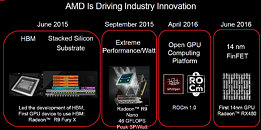
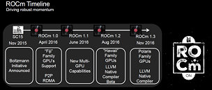
AMD on Monday announced their ROCm initiative. Introduced by AMD's Gregory Stoner, Senior Director for the Radeon Open Compute Initiative, ROCm stands for Radeon Open Compute platforM. This open-standard, high-performance, Hyper Scale computing platform stands on the shoulders of AMD's technological expertise and accomplishments, with cards like the Radeon R9 Nano achieving as much as 46 GFLOPS of peak single-precision performance per Watt.

The natural evolution of AMD's Boltzmann Initiative, ROCm grants developers and coders a platform which allows the leveraging of AMD's GPU solutions through a variety of popular programming languages, such as OpenCL, CUDA, ISO C++ and Python. AMD knows that the hardware is but a single piece in an ecosystem, and that having it without any supporting software is a recipe for failure. As such, AMD's ROCm stands as AMD's push towards HPC by leveraging both its hardware, as well as the support for open-standards and the conversion of otherwise proprietary code.

Sulon Q Powered by AMD, is the World's Most Advanced VR+AR Headset

As the 2016 Game Developer Conference kicks off, virtual and augmented reality continues to be top of mind for today's developers and consumers. And it should be. It represents the future of communication and computing, and the promise virtual reality has held for so long finally seems within grasp of today's technologies. Today, Sulon Technologies gets one step closer to that promise, unveiling a neak peek of the Sulon Q, the world's first and only all-in-one, tether-free, "wear and play" headset for virtual reality, augmented reality, and spatial computing.

On stage in front of more than 650 press and developers at the inaugural AMD Radeon "Capsaicin" event, I took the stage to give the world a glimpse of what we've been working on, showing off the forthcoming Sulon Q headset, and the intuitive experiences you can expect, including seamlessly transitioning from the real world to virtual worlds.

HSA Announces Publication of New Guide to Heterogeneous System Architecture

The Heterogeneous System Architecture (HSA) Foundation today announced publication of Heterogeneous System Architecture: A New Compute Platform Infrastructure (1st Edition), edited by Dr. Wen-Mei Hwu. The book, published by Elsevier Publishing (found here: here), offers a practical guide to understanding HSA, a standardized platform design that unlocks the performance and power efficiency of parallel computing engines found in most modern electronic devices.

"Heterogeneous computing is a key enabler of the next generation of compute environments, wherein entire systems will interconnect autonomously and in real time," said HSA Foundation President Dr. John Glossner. "Developers who are skilled in the use of this platform will have the upper hand in terms of design time, IP portability, power efficiency and performance."

To support these developers, the HSA Foundation working groups are rapidly standardizing tools and APIs for debug and profiling, creating guidelines for incorporating IP from multiple vendors into the same SoC, and much more. The Foundation released the v1.0 specification in March, and soon thereafter, companies including AMD, ARM, Imagination Technologies and MediaTek previewed their plans for rolling out the world's first products based on HSA.

AMD Announces PRO A-Series Processors for Business

AMD today introduced its most powerful line of AMD PRO A-Series mobile and desktop processors (formerly codenamed "Carrizo PRO" and "Godavari PRO") to deliver exceptional value and performance for today's challenging workloads. The new line of AMD PRO A-Series processors offer enhanced performance, reliability and opportunity to business users and IT decision makers and are designed for the future with Microsoft Windows 10. With its AMD PRO mobile processors, AMD powers some of the first-to-market Windows 10-enabled commercial notebook systems for those looking to upgrade.

"The innovative architecture of new AMD PRO processors delivers compelling performance to stay ahead of the evolving demands of business today," said Jim Anderson, senior vice president and general manager, computing and graphics, AMD. "Going PRO with AMD means unmatched dependability with platform stability, processor longevity and an opportunity for richer system configurations. AMD gives its customers choice and affordability to meet specific business needs, without compromising the ability to manage and maintain a secure, stable, and reliable environment."

AMD Unveils 6th Generation A-Series Processor

AMD today announced its 6th Generation A-Series Processor, the world's first high-performance Accelerated Processing Unit (APU) in a System-on-Chip (SoC) design. Previously codenamed "Carrizo," the 6th Generation AMD A-Series Processor takes advantage of extensive AMD processor and graphics IP enabling exceptional computing experiences not possible before. The 6th Generation AMD A-Series Processor is the most versatile notebook processor ever produced, built to excel at today's and tomorrow's consumer and business applications, delivering premium streaming entertainment, unmatched smooth online gaming, and innovative computing experiences, with all day unplugged performance.

The world's first high-performance Accelerated Processing Unit in a SoC design marks a number of technology firsts: the world's first High Efficiency Video Coding (HEVC) hardware decode support for notebooks, the first Heterogeneous Systems Architecture (HSA) 1.0-compliant design, and the first ARM TrustZone-capable high-performance APU. The new processor harnesses up to 12 Compute Cores -- 4 CPU + 8 GPU -- leveraging AMD "Excavator" cores and the third generation of AMD's award-winning Graphics Core Next (GCN) architecture. The result is a groundbreaking processor that boasts more than twice the battery life of its predecessor, up to 2x faster gaming performance than competitive processors, innovative computing experiences enabled through HSA, and a premium Microsoft Windows 10 experience with support for DirectX 12, adding up to an extraordinary experience for consumers.

AMD Announces New A-Series Desktop APUs

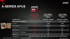
AMD today introduced the latest addition to its line of desktop A-Series processors, the A10-7870K APU, a refresh to the existing line of processors codenamed "Kaveri". The A10-7870K delivers a best-in-class experience for eSports and online gaming with superior performance, best-in-class efficiency in DirectX 12, and unique features. The new processor also delivers exceptional performance in modern workloads and is designed for the future with Microsoft Windows 10.

The latest iteration of the popular and powerful AMD A-Series APU family provides premium performance and multitasking powered by up to 12 compute cores (4 CPU + 8 GPU). The responsiveness and processing power of the A10-7870K APU enables an immersive user experience on Windows 10 PCs while offering an easy path for PC builders looking to upgrade to discrete-level graphics and faster processing at an afforadable price. The A10-7870K APU is available at e-tail now at a suggested price (SEP) of US $137, and through participating system builders.

AMD Awarded $32 Million for 'Extreme Scale' High-Performance Computing Research

AMD (NYSE: AMD) today announced that for the third straight year it was awarded research grants for development of critical technologies needed for extreme-scale computing in conjunction with projects associated with the U.S. Department of Energy (DOE) Extreme-Scale Computing Research and Development Program, known as "FastForward 2."

The two DOE awards, totaling more than $32 million, will fund research focused on exascale applications for AMD Accelerated Processing Units (APUs) based on the open-standard Heterogeneous System Architecture (HSA), as well as future memory systems to power a generation of exascale supercomputers capable of delivering 30-60 times more performance than today's fastest supercomputers.

AMD Announces Heterogeneous C++ AMP Language for Developers

AMD in collaboration with Microsoft today announced the release of C++ AMP version 1.2 -- an open source C++ compiler which implements version 1.2 of the open specification for C++ AMP, available on both Linux and Windows for the first time. The release represents another step forward toward AMD's goal of supporting cross-platform solutions, multiple programming languages and continued contributions to the open source community. The tool, which leverages Clang and LLVM, accelerates productivity and ease of use for developers wishing to harness the full power of modern heterogeneous platforms spanning servers, PCs and handheld devices.

"AMD has a consistent track record of enriching the developer experience, and we're proud to make the first open source implementation of C++ AMP available to enable greater performance and more power-efficient applications," said Manju Hegde, corporate vice president, Heterogeneous Applications and Solutions, AMD. "The cross-platform release is another step in strengthening AMD's developer solutions, allowing for increased productivity and accelerated applications through shared physical memory across the CPU and GPU on both Linux and Windows."

AMD Introduces New APUs for System Builder and DIY Market

AMD today introduced the new AMD A10-7800 Accelerated Processing Unit (APU) to the component channel. This 4th generation A-Series APU with 12 Compute Cores (4CPU + 8 GPU) unlocks the APU potential with Heterogeneous System Architecture (HSA) features, and boasts powerful AMD Radeon R7 Series graphics for outstanding performance across applications. Combined with AMD's acclaimed Mantle API, the AMD A10-7800 APU can enable accelerated performance across select AMD Gaming Evolved partner titles.

"The AMD A-Series APUs bring a superior level of gaming and compute experiences to the desktop PC," said Bernd Lienhard, corporate vice president and general manager, Client Business Unit, AMD. "With support for AMD's acclaimed Mantle API that simplifies game optimizations for programmers and developers to unlock unprecedented levels of gaming performance transforming the world of game development to help bring better, faster games to the PC."

AMD Announces Its Most Advanced Mobile APU for Consumer and Commercial Notebooks

AMD (NYSE: AMD) today introduced its new 2014 Performance Mobile APUs designed for ultrathin and high-performance mobile PCs, bringing the features and capabilities of the popular and powerful AMD A-Series APU family (codenamed "Kaveri") to power-efficient notebooks for both personal and professional use. The new mobile APUs mark the debut of Heterogeneous System Architecture (HSA) features and Graphics Core Next (GCN) Architecture for mobile devices, establishing them as AMD's most advanced mobile APUs to-date. Notebook and desktop systems powered by AMD's entire 2014 APU lineup, including systems from Acer, Asus, Dell, HP, Lenovo, Samsung, Toshiba and others also debuted at COMPUTEX TAIPEI 2014.

"AMD takes a major step forward today on our journey to transform and enhance the computing experience with the launch of the 2014 Performance Mobile APU family," said Bernd Lienhard, corporate vice president and general manager, Client Business Unit, AMD. "With a combination of superior total compute performance, stunning graphics and efficient power use alongside industry-first technologies, these new APUs set a new bar for cutting-edge consumer and commercial PCs."
The announcement of the 2014 Performance Mobile APU family features AMD's first FX-branded enthusiast-class APU for notebooks, and follows the recent introduction of AMD's 2014 Low-Power and Mainstream APUs.

AMD Announces 2nd Generation Embedded R-Series APUs and CPUs

AMD today announced the 2nd generation AMD Embedded R-series accelerated processing unit (APU) and CPU family (previously codenamed "Bald Eagle") for embedded applications. The new solutions are targeted at gaming machines, medical imaging, digital signage, industrial control and automation (IC&A), communications and networking infrastructure that require industry-leading compute and graphics processing technology.

"When it comes to compute performance, graphics performance and performance-per-watt, the 2nd generation AMD Embedded R-series family is unique in the embedded market," said Scott Aylor, corporate vice president and general manager, AMD Embedded Solutions. "The addition of HSA, GCN and power management features enables our customers to create a new world of intelligent, interactive and immersive embedded devices."

AMD to Research Interconnect Architectures for High-Performance Computing

AMD today announced that it was selected for an award of $3.1 million for a research project associated with the U.S. Department of Energy (DOE) Extreme-Scale Computing Research and Development Program, known as "DesignForward." The DOE award is an expansion of work started as part of another two-year award AMD received in 2012 called "FastForward." The FastForward award aims to accelerate the research and development of processor and memory technologies needed to support extreme-scale computing. The DesignForward award supports the research of the interconnect architectures and technologies needed to support the data transfer capabilities in extreme-scale computing environments.

DesignForward is a jointly funded collaboration between the DOE Office of Science and the U.S. National Nuclear Security Administration (NNSA) to accelerate the research and development of critical technologies needed for extreme-scale computing, on the path toward Exascale computing. Exascale supercomputers are expected to be capable of performing computation hundreds of times faster than today's fastest computers, with only slightly higher power utilization.

AMD Debuts New SDK, Tools and Libraries, for Heterogeneous Computing Developers

AMD kicked off its 2013 Developer Summit (APU13) today, announcing a new unified Software Development Kit (SDK,) an improved CodeXL tool suite with added features and support for the latest AMD hardware, and added heterogeneous acceleration in popular Open Source libraries. Together, these tools provide a substantial step forward in productivity and ease-of-use for developers wishing to harness the full power of modern heterogeneous platforms spanning form servers to PCs to handheld devices.

"Developers are essential to our mission of realizing the full potential of modern computing technologies," said Manju Hegde, corporate vice president, Heterogeneous Solutions, AMD. "Enriching the developer experience by harnessing these technologies is a critical part of AMD's mission to accelerate developer adoption."

AMD Enables Server APU Software to Reimagine the Server

AMD today announced it is enabling its accelerated processing units (APU) for next-generation servers through important advancements in software tools developed by AMD and in collaboration with technology partners and the open source community. In his keynote address at APU13, AMD Corporate Fellow Phil Rogers highlighted the significant progress AMD has made in both developing software internally and empowering others to develop software to take advantage of the capabilities of AMD APU technology, which combines industry leading AMD Radeon graphics processing engines with x86 computational processing on a single chip.

"Servers must be efficient, scalable and adaptable to meet the compute characteristics of new and changing workloads. Software applications that leverage server APUs are designed to drive highly efficient, low-power, dense server solutions optimized for highly parallel and multimedia workloads," said Suresh Gopalakrishnan, corporate vice president and general manager of the Server Business Unit, AMD. "We have evolved our processor roadmap to support this opportunity, and now we are showcasing how the APU software ecosystem is gaining momentum and what developers can do to participate."

HSA Foundation Announces First Specification

The HSA Foundation has released Version 0.95 of its Programmer's Reference Manual. The HSA (Heterogeneous System Architecture) Foundation is a not-for-profit consortium dedicated to developing architecture specifications that unlock the performance and power efficiency of the parallel computing engines found in most modern devices. This is the first output from the HSA Foundation, who have been collaborating on this project since its founding in June 2012. It represents an important step in the development of the HSA Foundation's ecosystem because it enables software partners to develop libraries, tools and middleware and to code high performance kernels.

The Programmer's Reference Manual provides a standardized method of accessing all available computing resources in HSA-compliant systems. This enables a wide range of system resources to cooperate on parallelizable tasks. It has been specifically designed to perform in the most energy efficient way without compromising on performance. The goal is to enable a heterogeneous architecture that is easy to program, opens up new and rich user experiences and improves performance and quality of service, whilst reducing energy consumption.

Tensilica Joins HSA Foundation

Tensilica, Inc. today announced that it has joined the HSA (Heterogeneous System Architecture) Foundation, a not-for-profit consortium dedicated to developing architecture specifications that will unlock the performance and power efficiency of parallel computing engines found in many modern devices. Tensilica will contribute its years of experience assisting customers in bringing heterogeneous multicore SoC (system-on-chip) designs to market to the development and promotion of standards for parallel computing.

"Tensilica is a long-established leader in multicore technology, delivering unique solutions that enable both control plane and compute-intensive dataplane functions," stated Steve Roddy, Tensilica's vice president of product marketing and business development. "Tensilica customers today use multiple Tensilica processors for diverse functions such as audio offload, wireless baseband, image processing and general purpose control. We welcome the efforts and ambitions of the HSA to bring standards to the market that will greatly facilitate innovation in embedded applications."
Return to Keyword Browsing
Jan 21st, 2025 20:07 EST change timezone

New Forum Posts

Popular Reviews

Controversial News Posts