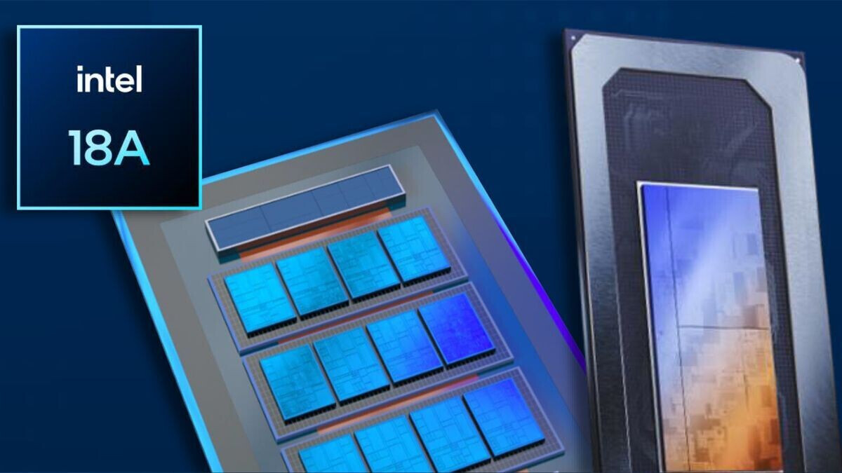
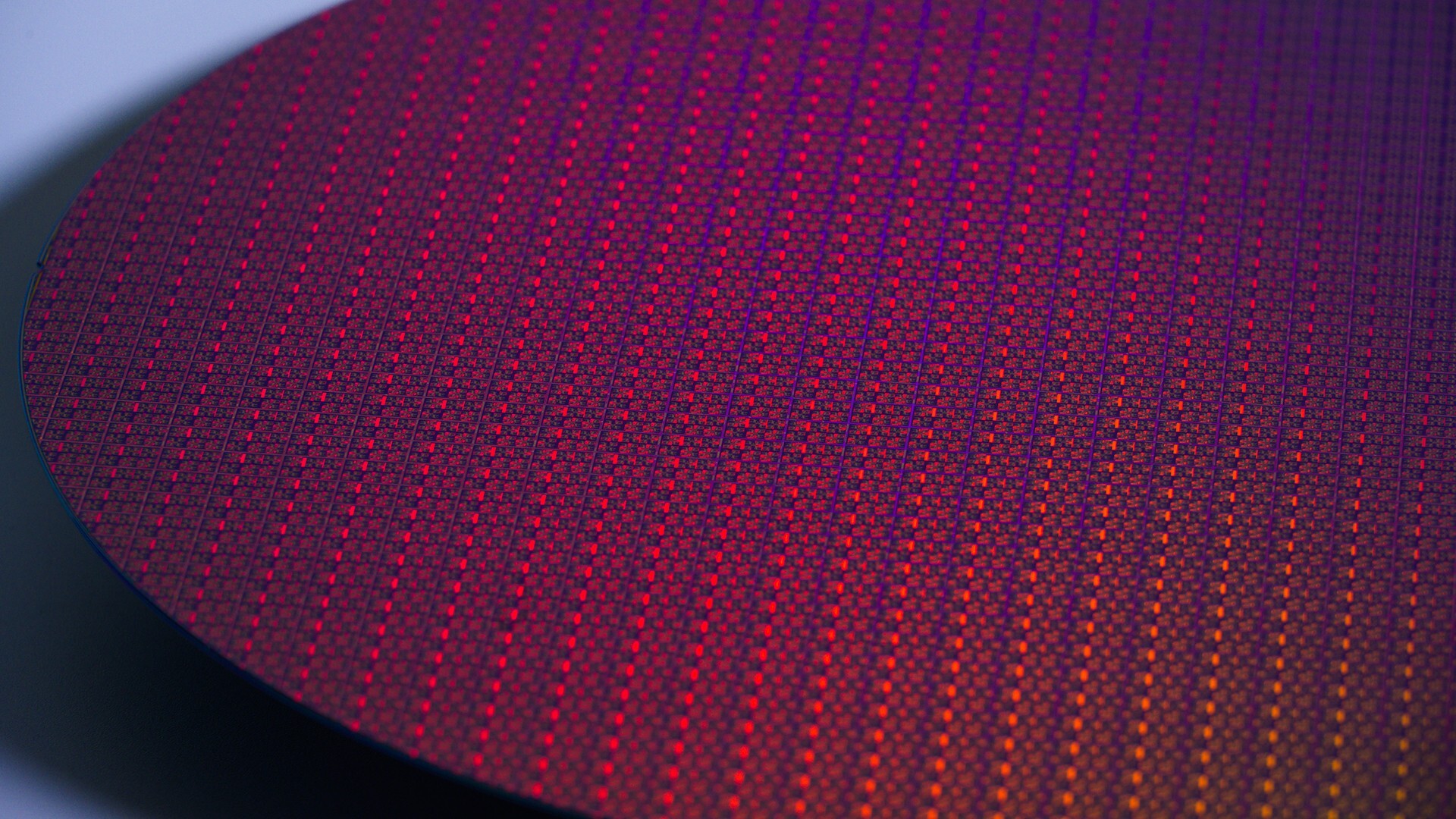
Intel's 18A Node Outperforms TSMC N2 and Samsung SF2 in 2 nm Performance Class
Intel's 18A node isn't all about yields and density (which are still very important factors) but also performance. According to Taiwanese media 3C News, citing TechInsights research and calculations, the new leader of node performance is Intel 18A. On a custom scale used by TechInsights, Intel 18A gets a 2.53 score, while the performance score of TSMC N2 is 2.27, and the performance score of Samsung SF2 is 2.19. This is all among two nm-class nodes, where Intel leads the category. Being the first node with a Backside Power Delivery Network (BSPDN), it will appear in the Panther Lake CPUs in late 2025 for testing and early 2026 for shipments. This new power architecture boosts layout efficiency and component utilization by 5-10%, lowers interconnect resistance, and enhances ISO power performance by up to 4%, thanks to a significant drop in intrinsic resistance versus traditional front‑end power routing. Relative to its predecessor, Intel 3, the 18A process delivers a 15% improvement in performance per watt and packs 30% more transistors into the same area.
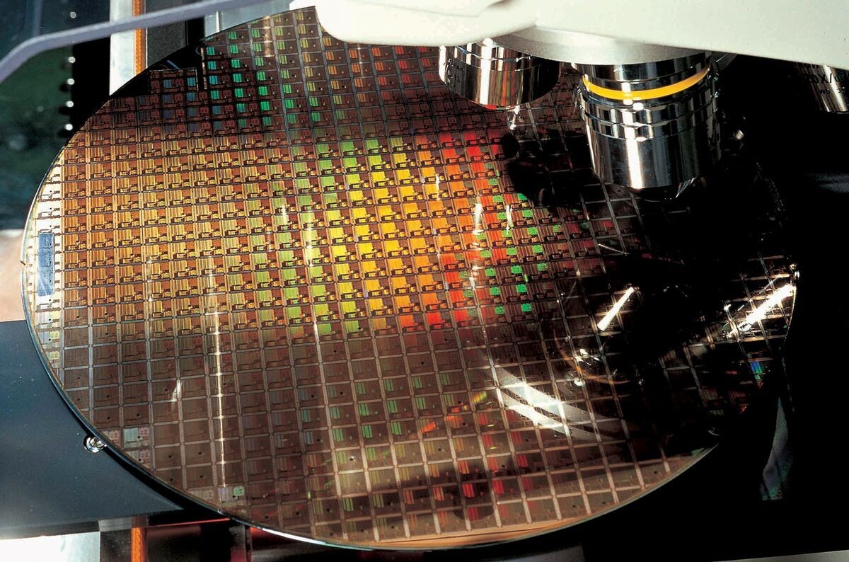
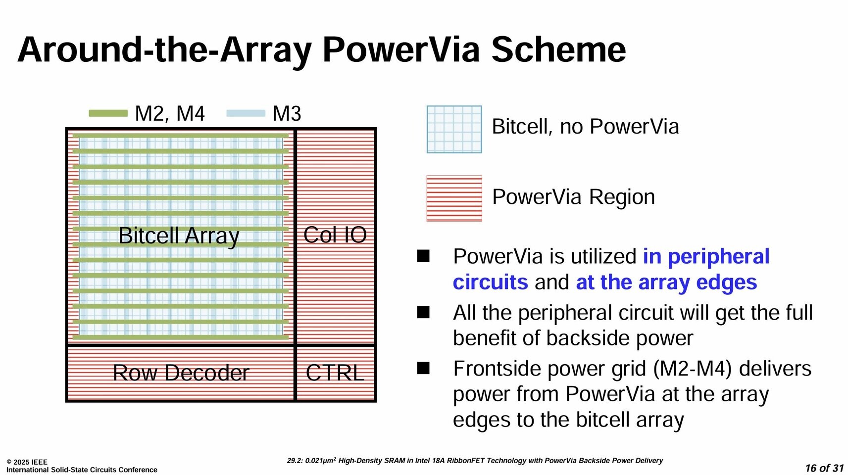
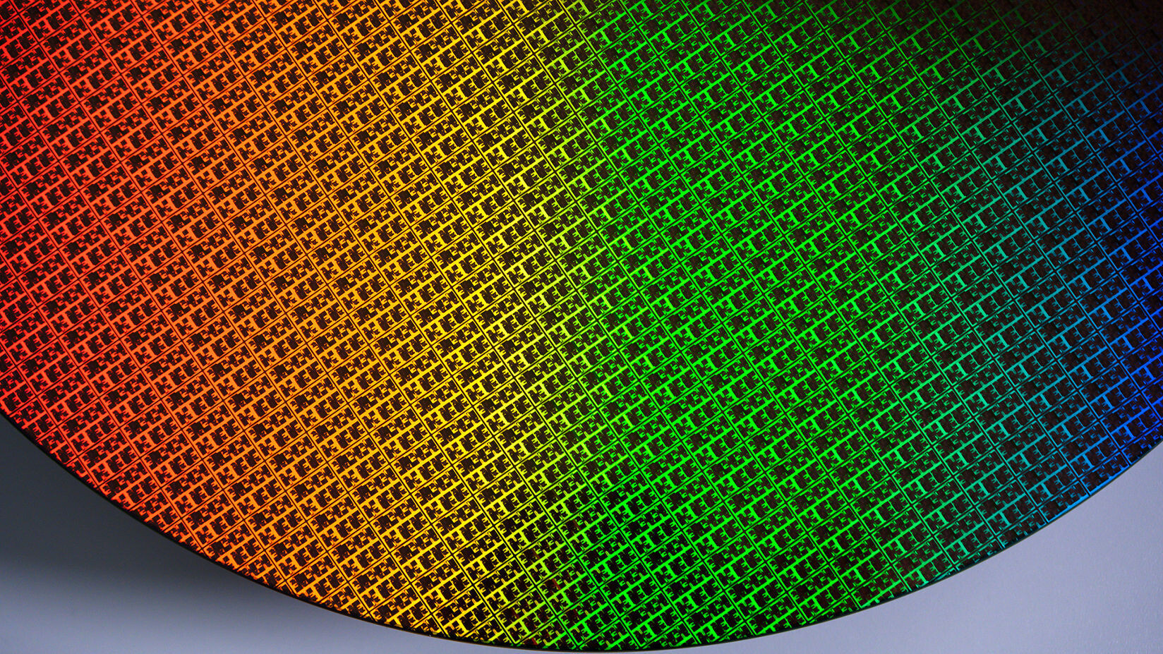
Featuring RibbonFET design, it has entered risk production. According to Intel, "This final stage is about stress-testing volume manufacturing before scaling up to high volume in the second half of 2025." When it comes to other aspects like SRAM density, high‑performance SRAM cells shrank from 0.03 µm² in Intel 3 to 0.023 µm² in Intel 18A, while high‑density cells contracted to 0.021 µm², reflecting scaling factors of 0.77 and 0.88 respectively and defying previous assumptions that SRAM scaling had plateaued. Intel's innovative "around‑the‑array" PowerVia approach addresses voltage drops and interference by routing power vias to I/O, control, and decoder circuits, freeing up the bit‑cell area from frontal power supplies. The result is a 38.1 Mbit/mm² macro bit density, positioning Intel to rival TSMC's N2. All this, combined with BSPDN, is shaping up a powerful node. We can't wait to get our hands on some 18A silicon in the future and run it through our labs for testing.
Featuring RibbonFET design, it has entered risk production. According to Intel, "This final stage is about stress-testing volume manufacturing before scaling up to high volume in the second half of 2025." When it comes to other aspects like SRAM density, high‑performance SRAM cells shrank from 0.03 µm² in Intel 3 to 0.023 µm² in Intel 18A, while high‑density cells contracted to 0.021 µm², reflecting scaling factors of 0.77 and 0.88 respectively and defying previous assumptions that SRAM scaling had plateaued. Intel's innovative "around‑the‑array" PowerVia approach addresses voltage drops and interference by routing power vias to I/O, control, and decoder circuits, freeing up the bit‑cell area from frontal power supplies. The result is a 38.1 Mbit/mm² macro bit density, positioning Intel to rival TSMC's N2. All this, combined with BSPDN, is shaping up a powerful node. We can't wait to get our hands on some 18A silicon in the future and run it through our labs for testing.