Thursday, February 20th 2025

Intel 18A Node SRAM Density On-Par with TSMC, Backside Power Delivery a Big Bonus
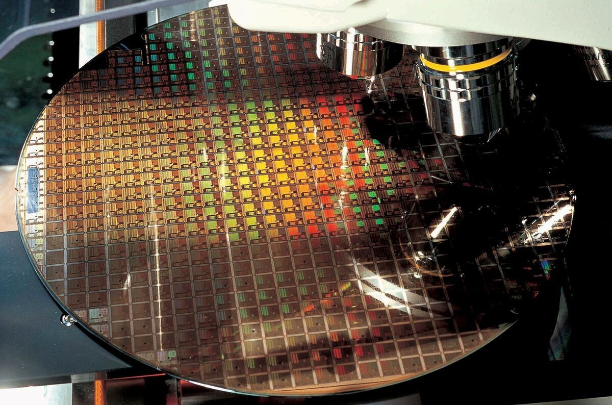
Intel has unveiled some interesting advances in semiconductor manufacturing at the International Solid-State Circuits Conference (ISSCC), showcasing the capabilities of its highly anticipated Intel 18A process technology. The presentation highlighted significant improvements in SRAM bit cell density. The PowerVia system, coupled with RibbonFET (GAA) transistors, is at the heart of Intel's node. The company demonstrated solid progress with their high-performance SRAM cells, achieving a reduction from 0.03 µm² in Intel 3 to 0.023 µm² in Intel 18A. High-density cells showed similar improvement, shrinking to 0.021 µm². These advancements represent scaling factors of 0.77 and 0.88 respectively, which are significant achievements in SRAM technology, once thought to be done with scaling benefits.
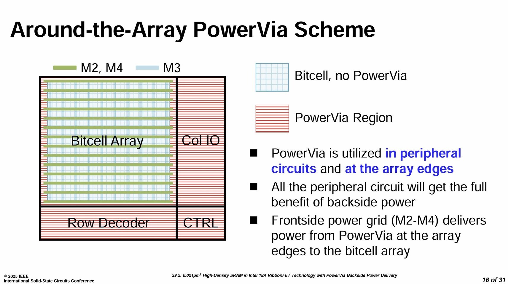
Implementing PowerVia technology is an Intel-first approach to addressing voltage drops and interference in processor logic areas. Using an "around the array" scheme, Intel strategically applies PowerVias to I/O, control, and decoder elements while optimizing bit cell design without a frontal power supply. The macro bit density of 38.1 MBit/mm² achieved by Intel 18A puts the company in a strong competitive position. While TSMC reported matching figures with their N2 process, Intel's comprehensive approach with 18A, combining PowerVia and GAA transistors, could challenge Smausng and TSMC, with long-term aspirations to compete for premium clients currently served by TSMC, including giants like NVIDIA, Apple, and AMD.


Sources:
Ian Cutress, via HardwareLuxx
Implementing PowerVia technology is an Intel-first approach to addressing voltage drops and interference in processor logic areas. Using an "around the array" scheme, Intel strategically applies PowerVias to I/O, control, and decoder elements while optimizing bit cell design without a frontal power supply. The macro bit density of 38.1 MBit/mm² achieved by Intel 18A puts the company in a strong competitive position. While TSMC reported matching figures with their N2 process, Intel's comprehensive approach with 18A, combining PowerVia and GAA transistors, could challenge Smausng and TSMC, with long-term aspirations to compete for premium clients currently served by TSMC, including giants like NVIDIA, Apple, and AMD.

14 Comments on Intel 18A Node SRAM Density On-Par with TSMC, Backside Power Delivery a Big Bonus
Arp arp arp
The thing that amused me the most is Intel naming AMD as a giant. :)