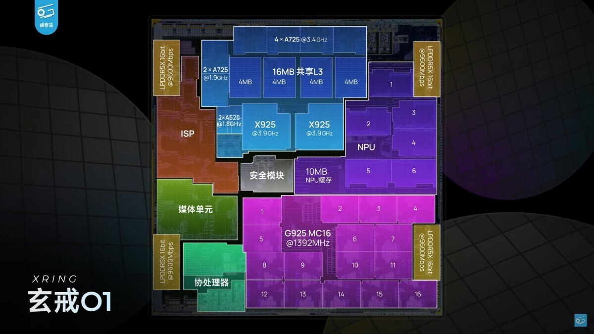
Xiaomi XRING SoCs Possibly Limited to 3 nm, New Restrictions Affecting EDA Software Supply
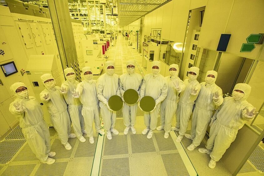
According to the Financial Times, new restrictions—affecting the supply of Electronic Design Automation (EDA) software suites to Chinese companies—will cause major disruption within the domestic chip design industry. The US government's latest trade amendments are expected to impact Xiaomi and its freshly launched flagship XRING mobile chip family; the first iteration is a compelling first-party effort. Unlike many Chinese tech firms, the popular smartphone specialist can access pretty advanced TSMC node processes. Xiaomi's CEO—Lei Jun—announced his team's 3 nm design during pre-launch preview events.
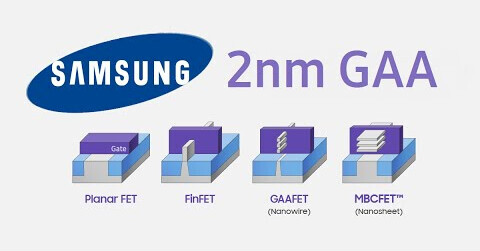
Days later, closer analysis indicated a selection of TSMC's "N3E" node process. Digital Chat Station—a noted smartphone industry expert—summarized an uncertain future: "under this ban (of EDA tools), XRING chips will not be breaking through a 2 nm barrier, and can only revolve around the (current 'N3E') 3 nm node for a long time. XRING O1 will also be the only time in recent years that it can be on par with current-gen (proprietary) Apple, Qualcomm, and MediaTek mobile chipsets." Crucially, EDA software plays an important role in creating Gate All Around Field Effect Transistor (GAAFET) structures. TSMC's upcoming 2 nm node process is a GAA product. Tom's Hardware believes that several big Chinese tech players, including Huawei, are in the process of developing in-house EDA tools. Not long after unveiling their XRING flagship, Xiaomi outlined an extended Qualcomm chip deal.


Days later, closer analysis indicated a selection of TSMC's "N3E" node process. Digital Chat Station—a noted smartphone industry expert—summarized an uncertain future: "under this ban (of EDA tools), XRING chips will not be breaking through a 2 nm barrier, and can only revolve around the (current 'N3E') 3 nm node for a long time. XRING O1 will also be the only time in recent years that it can be on par with current-gen (proprietary) Apple, Qualcomm, and MediaTek mobile chipsets." Crucially, EDA software plays an important role in creating Gate All Around Field Effect Transistor (GAAFET) structures. TSMC's upcoming 2 nm node process is a GAA product. Tom's Hardware believes that several big Chinese tech players, including Huawei, are in the process of developing in-house EDA tools. Not long after unveiling their XRING flagship, Xiaomi outlined an extended Qualcomm chip deal.