Friday, February 28th 2025

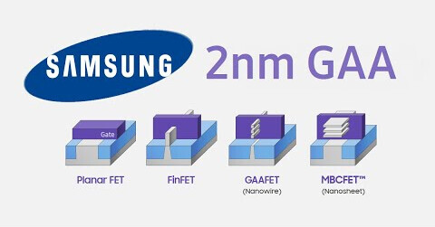
Samsung Reportedly Progressing Well with 2 nm GAA Yields, Late 2025 Mass Production Phase Looms
Samsung's foundry operation has experienced many setbacks over the past six months, according to a steady feed of insider reports. Last November, industry moles leaked details of an apparent abandonment of the company's 3 nm Gate-All-Around (GAA) process. Significant yield problems prompted an alleged shift into 2 nm territories, with a next-gen flagship Exynos mobile processor linked to this cutting-edge node. According to a mid-week Chosun Daily article, Samsung and its main rival—TSMC—are in a race to establish decent yields of 2 nm wafers, ahead of predicted "late 2025" mass production kick-offs. The publication's inside track points to the Taiwanese foundry making the most progress (with an estimated 60%), but watchdogs warn that it is too early to bet against the South Korean competitor.
Despite murmurs of current 20 - 30% yields, the Samsung's Hwaseong facility is touted to make "smooth" progress over the coming months. Chosun's sources believe that Samsung engineers struggled to get 3 nm GAA "up to snuff," spending around three years on development endeavors (in vain). In comparison, the making of 2 nm GAA is reported to be less bumpy. A fully upgraded "S3" foundry line is expected to come online by the fourth quarter of this year. An unnamed insider commented on rumors of better than anticipated forward motion chez Samsung Electronics: "there are positive aspects to this as it has shown technological improvements, such as the recent increase in the yield of its 4 nm process by up to 80%." Recent-ish reports suggest that foundry teams have dealt with budget cuts, as well as mounting pressure from company leadership to hit deadlines.


Sources:
Chosun Business News, Wccftech, EDN (graphic source), Jukanlosreve Tweet
Despite murmurs of current 20 - 30% yields, the Samsung's Hwaseong facility is touted to make "smooth" progress over the coming months. Chosun's sources believe that Samsung engineers struggled to get 3 nm GAA "up to snuff," spending around three years on development endeavors (in vain). In comparison, the making of 2 nm GAA is reported to be less bumpy. A fully upgraded "S3" foundry line is expected to come online by the fourth quarter of this year. An unnamed insider commented on rumors of better than anticipated forward motion chez Samsung Electronics: "there are positive aspects to this as it has shown technological improvements, such as the recent increase in the yield of its 4 nm process by up to 80%." Recent-ish reports suggest that foundry teams have dealt with budget cuts, as well as mounting pressure from company leadership to hit deadlines.


2 Comments on Samsung Reportedly Progressing Well with 2 nm GAA Yields, Late 2025 Mass Production Phase Looms
None of them are *exactly* the same, but you get my point. They are all trying to get that approximate level of p/p/a (different ratios) to a practical yield...Don't put a ton of stock into the node name.
Beyond that is pretty expensive to develop (w/ little advancement), so that's where I think a lot of people are going to see returns diminish to the point they don't upgrade most of their stuff (for a long time).
In some ways that sucks for us (as nerds that love watching this stuff advance), in some ways I'm ready to invest in something that if it's going to be expensive, it least it will last for a good, long while.