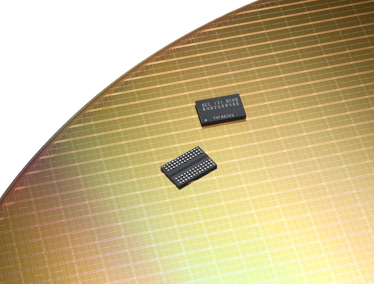
Samsung Reportedly Achieves 70% Yields for Its 1c DRAM Technology
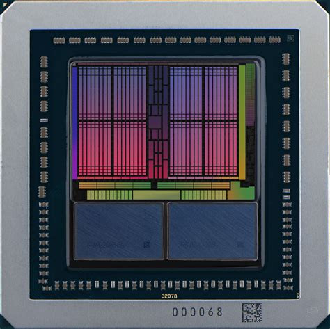
Samsung has achieved better production results for its advanced memory technology, according to Sedaily, as cited by TrendForce. The company's sixth-generation 10 nm DRAM, called 1c DRAM, now shows yield rates of 50-70% in testing. This represents a significant improvement from last year's results, which were below 30%. Samsung takes a different path from its rivals, while SK Hynix and Micron stick with 1b DRAM technology for HBM4 products, Samsung opts to create the newer 1c DRAM. This choice comes with more risk; however, it might bring bigger rewards, as the improved production rates enable Samsung to expand its manufacturing operations. The company plans to increase 1c DRAM production at its Hwaseong and Pyeongtaek facilities with expansion activities expected to begin before the end of this year.
These developments also support Samsung's HBM4 production schedule since the company aims to begin mass production of HBM4 products later this year. Yet, experts in the field point out that the product is still in its early stages and needs ongoing monitoring. Samsung planned to begin mass-producing sixth-gen 10 nm DRAM by late 2024. Instead, the company chose to remake the chip's design. This decision caused delays of more than one year however it was made to achieve better performance and yields. The new DRAM products will be manufactured at Samsung's Pyeongtaek Line 4 facility as these chips will serve both mobile and server applications. Separately, HBM4-related production will take place at Pyeongtaek Line 3.
These developments also support Samsung's HBM4 production schedule since the company aims to begin mass production of HBM4 products later this year. Yet, experts in the field point out that the product is still in its early stages and needs ongoing monitoring. Samsung planned to begin mass-producing sixth-gen 10 nm DRAM by late 2024. Instead, the company chose to remake the chip's design. This decision caused delays of more than one year however it was made to achieve better performance and yields. The new DRAM products will be manufactured at Samsung's Pyeongtaek Line 4 facility as these chips will serve both mobile and server applications. Separately, HBM4-related production will take place at Pyeongtaek Line 3.