Rapidus Achieves Significant Milestone with Prototyping of Leading-Edge 2nm GAA Transistors
Rapidus Corporation, a manufacturer of advanced logic semiconductors, today announced that prototyping has started for its 2 nm gate-all-around (GAA) transistor structure at Rapidus Innovative Integration for Manufacturing (IIM-1) foundry. The prototype wafers also started to obtain their electrical characteristics. Rapidus new IIM-1 foundry represents a significant advancement over the traditional foundry model. The company is re-imagining how semiconductor factories should think, learn, adapt and optimize processes in real time through cutting-edge methods and technology including:
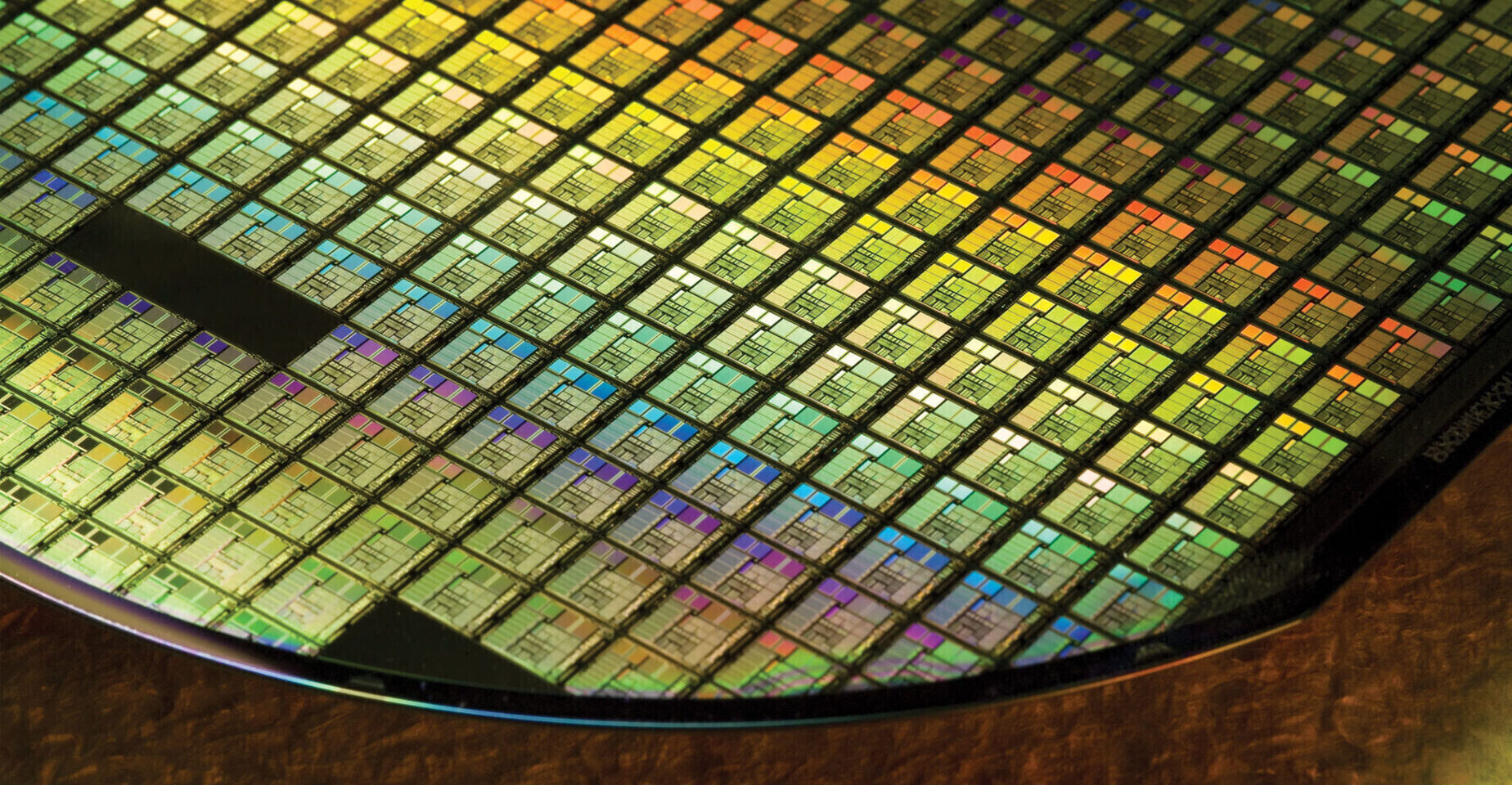
Fully single-wafer front-end processing: In a single-wafer process, adjustments can be made to a single wafer, inspected and if successful, applied to all subsequent wafers. Single wafer captures more data, enabling AI models to be trained to improve wafer production and increase yields. Rapidus is one of the first companies that will commercialize fully single-wafer processing, which is central to its Rapid and Unified Manufacturing Service (RUMs).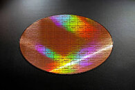


Fully single-wafer front-end processing: In a single-wafer process, adjustments can be made to a single wafer, inspected and if successful, applied to all subsequent wafers. Single wafer captures more data, enabling AI models to be trained to improve wafer production and increase yields. Rapidus is one of the first companies that will commercialize fully single-wafer processing, which is central to its Rapid and Unified Manufacturing Service (RUMs).