Samsung Electronics Announces Fourth Quarter and FY 2022 Results, Profits at an 8-year Low
Samsung Electronics today reported financial results for the fourth quarter and the fiscal year 2022. The Company posted KRW 70.46 trillion in consolidated revenue and KRW 4.31 trillion in operating profit in the quarter ended December 31, 2022. For the full year, it reported 302.23 trillion in annual revenue, a record high and KRW 43.38 trillion in operating profit.
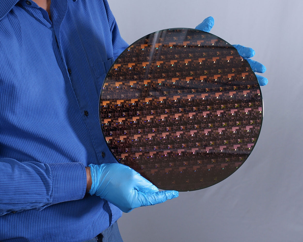
The business environment deteriorated significantly in the fourth quarter due to weak demand amid a global economic slowdown. Earnings at the Memory Business decreased sharply as prices fell and customers continued to adjust inventory. The System LSI Business also saw a decline in earnings as sales of key products were weighed down by inventory adjustments in the industry. The Foundry Business posted a new record for quarterly revenue while profit increased year-on-year on the back of advanced node capacity expansion as well as customer base and application area diversification.
The business environment deteriorated significantly in the fourth quarter due to weak demand amid a global economic slowdown. Earnings at the Memory Business decreased sharply as prices fell and customers continued to adjust inventory. The System LSI Business also saw a decline in earnings as sales of key products were weighed down by inventory adjustments in the industry. The Foundry Business posted a new record for quarterly revenue while profit increased year-on-year on the back of advanced node capacity expansion as well as customer base and application area diversification.