News Posts matching #PowerVia

Return to Keyword Browsing

Intel Showcases 18A Node Performance: 25% Faster and 40% Lower Power Draw

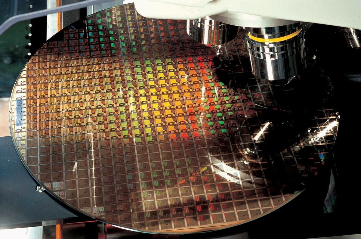
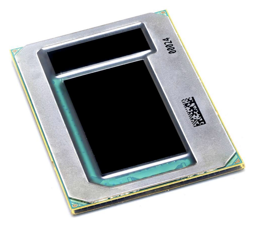
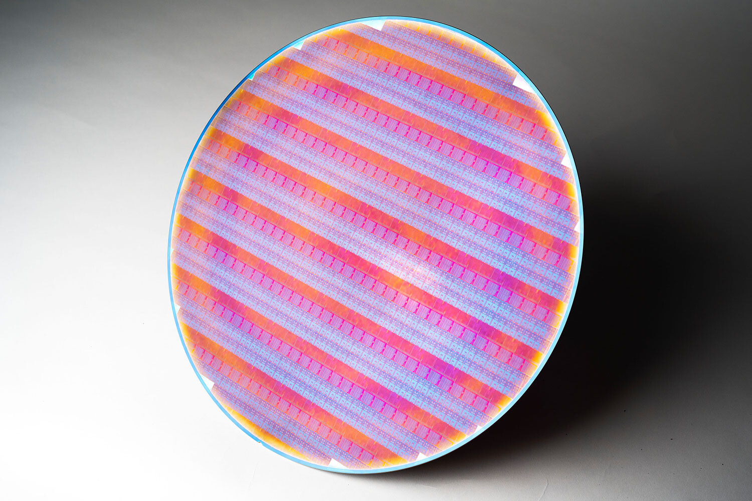
Intel's presentation at the VLSI Symposium in Japan offered a detailed look at the upcoming Intel 18A process, which is set to enter mass production in the second half of 2025. This node combines Gate-All-Around transistors with the PowerVia backside power delivery network, resulting in a completely new metal stack architecture. By routing power through the rear of the die, Intel has been able to tighten interconnect pitches on critical layers while relaxing spacing on the top layer, improving yield and simplifying fabrication. In standardized power, performance, and area tests on an Arm core sub-block, Intel 18A demonstrated roughly 15% higher performance at the same power draw compared to Intel 3. When operating at 1.1 volts, clock speeds increase by up to 25% without incurring additional energy costs, and at around 0.75 volts, performance can rise by 18%, or power consumption can drop by nearly 40%.

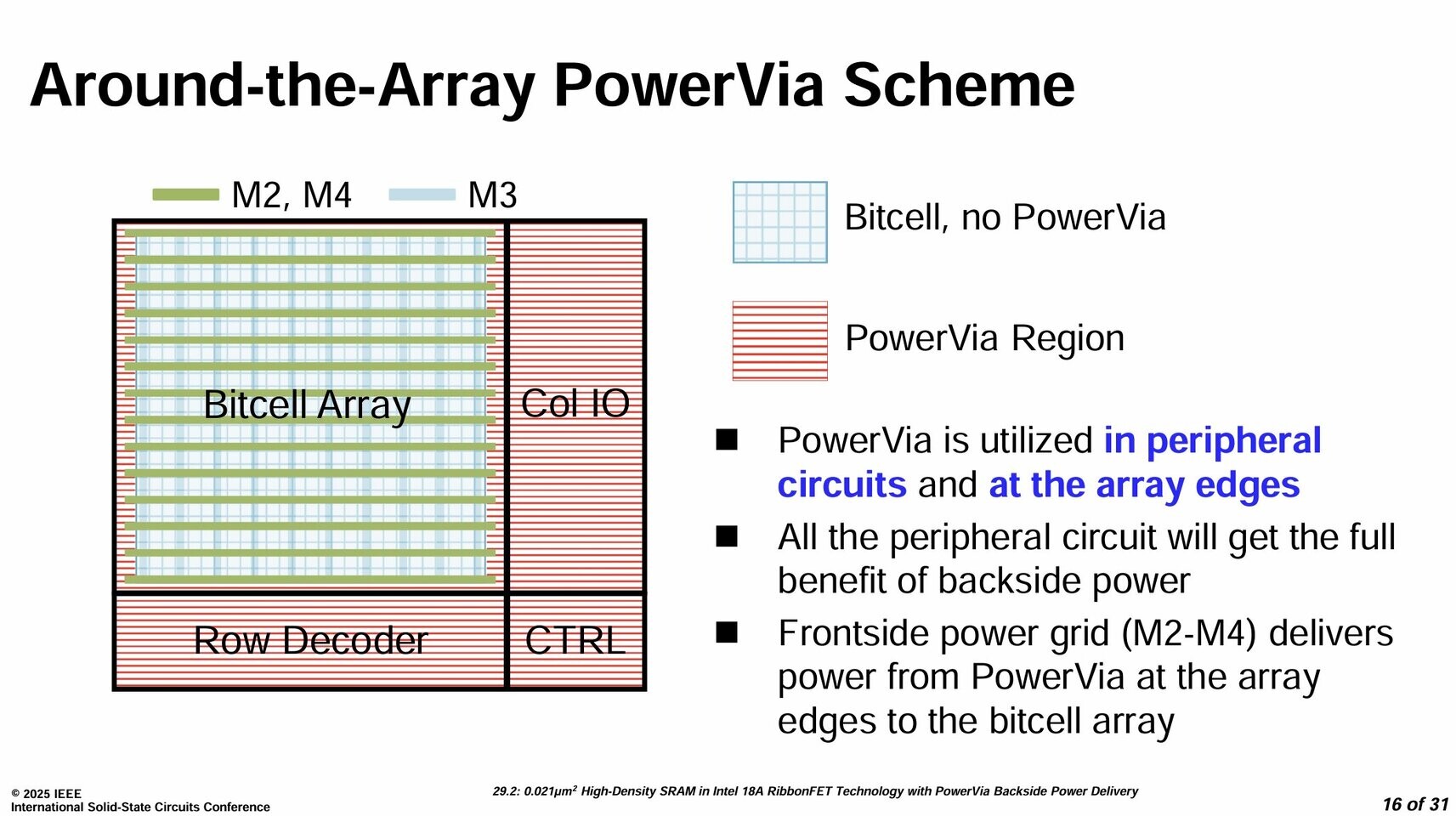
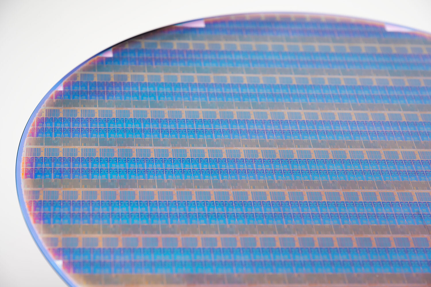
Under the hood, the process features significant cell height reductions: performance‑tuned cells measure 180 nanometers tall, while high‑density designs sit at 160 nanometers, both smaller than their predecessors. The front‑side metal layers have been reduced from between 12 and 19 on Intel 3 to between 11 and 16 on Intel 18A, with three additional rear metal layers added for PowerVia support. Pitches on layers M1 through M10 have been tightened from as much as 60 nanometers down to 32 nanometers before easing again in the upper layers. Low-NA EUV exposure is used on layers M0 through M4, cutting the number of masks required by 44% and simplifying the manufacturing flow. Intel plans to debut 18A in its low‑power "Panther Lake" compute chiplet and the efficiency‑core‑only Clearwater Forest Xeon 7 family. A cost-optimized 17-layer variant, a balanced 21-layer option, and a performance-focused 22-layer configuration will address different market segments.

Siemens and Intel Foundry Collaborates on Integrated Circuits and Advanced Packaging Solutions for 2D and 3D IC

Siemens Digital Industries Software today announced that its continued collaboration with Intel Foundry has resulted in multiple product certifications, updated foundry reference flows, and additional technology enablement leveraging the foundry's leading-edge technologies for next-generation integrated circuits (IC) and advanced packaging. Siemens is a founding partner of the Intel Foundry Accelerator Chiplet Alliance - enabling a new and compelling solution for 3D IC and chiplet offerings to a breadth of semiconductor market verticals.

Intel 18A Certification Achievements
Siemens' industry-leading Calibre nmPlatform tool is now certified for the latest Intel 18A production Process Design Kit (PDK). Intel 18A represents a significant technological leap forward, featuring innovative RibbonFET Gate-all-around transistors and the industry's first PowerVia backside power delivery. This Calibre certification allows mutual customers to continue leveraging the Calibre nmPlatform tool as their industry-standard sign-off solution with Intel Foundry's most advanced manufacturing process, accelerating time-to-market for next-generation chip designs.

Intel 14A Node Debuts "Turbo Cells" to Boost Frequency and Cut Power

During Intel's Foundry Direct Connect symposium in San Jose, where Intel confirmed the ramp of the 18A node at the Arizona fab, the company also announced Intel has achieved a significant advancement in its future node development with the announcement of "turbo cell" technology for its upcoming 14A process. Now slated for production in 2027, this progress supports Intel's objective of introducing five process nodes within a four-year period. The 18A node is presently in risk production and incorporates RibbonFET gate-all-around transistors along with PowerVia, Intel's backside power-delivery architecture. Intel anticipates transitioning 18A to full-volume manufacturing later this year, thereby internalizing greater chiplet assembly work that was previously outsourced for designs such as Lunar Lake.

For the upcoming 14A process, it combines second-generation RibbonFET with PowerDirect, the company's enhanced power network. When implemented using High-NA EUV lithography, Intel projects a performance-per-watt gain of between 15 and 20 percent over the 18A process. Of particular interest is the introduction of turbo cells. These specialized standard-cell libraries enable designers to integrate both high-performance and energy-efficient cells within a single design block. Such flexibility permits precise optimization of chip speed, power consumption, and die area to meet diverse application requirements. In practical terms, turbo cells are expected to elevate peak CPU frequencies and accelerate critical GPU pathways without incurring substantial energy penalties. Intel has already distributed its PDK for the 14A node to prospective customers for feedback, with multiple partners already planning test-chip tape-outs. Complementing these advances, the company will employ advanced packaging technologies, including Foveros 3D stacking and EMIB, and a new high-bandwidth EMIB-T variant to integrate 14A and 18A dies within unified hybrid packages.

Ansys Thermal and Multiphysics Solutions Certified for Intel 18A Process and 3D-IC Designs

Ansys today announced thermal and multiphysics signoff tool certifications for designs manufactured with Intel 18A process technology. These certifications help ensure functionality and reliability of advanced semiconductor systems for the most demanding applications—including AI chips, graphic processing units (GPUs), and high-performance computing (HPC) products. Intel Foundry and Ansys have also enabled a comprehensive multiphysics signoff analysis flow for Intel Foundry's EMIB technology used for creating multi-die 3D integrated circuit (3D-IC) systems.

Recognized as industry-leading solutions, RedHawk-SC and Totem deliver speed, accuracy, and capacity to analyze the power integrity and reliability of Intel 18A RibbonFET Gate-all-around (GAA) transistors with PowerVia backside power delivery. For scalable electromagnetic analysis, Ansys is introducing HFSS-IC Pro, a new addition to the HFSS-IC product family. HFSS-IC Pro is certified for modeling on-chip electromagnetic integrity in radio frequency chips, Wi-Fi, 5G/6G, and other telecommunication applications made with the Intel 18A process node.

Intel Foundry Gathers Customers and Partners, Outlines Priorities

Today at Intel Foundry Direct Connect, the company will share progress on multiple generations of its core process and advanced packaging technologies. The company will also announce new ecosystem programs and partnerships, and welcome industry leaders to discuss how a systems foundry approach enables collaboration with partners and unlocks innovation for customers.

Intel CEO Lip-Bu Tan will open the event by discussing Intel Foundry's progress and priorities as the company drives the next phase of its foundry strategy. Naga Chandrasekaran, Intel Foundry chief technology and operations officer, and Kevin O'Buckley, general manager of Foundry Services, will also deliver keynotes during the morning session, sharing process and advanced packaging news while highlighting Intel Foundry's globally diverse manufacturing and supply chain.

Cadence Expands Design IP Portfolio Optimized for Intel 18A and Intel 18A-P Technologies

Cadence today announced a significant expansion of its portfolio of design IP optimized for Intel 18A and Intel 18A-P technologies and certification of Cadence digital and analog/custom design solutions for the latest Intel 18A process design kit (PDK). These advancements are being showcased today at Intel Foundry Direct Connect, underscoring Cadence's continued leadership in driving industry innovation for artificial intelligence and machine learning (AI/ML), high-performance computing (HPC) and advanced mobility applications through its strategic partnership with Intel Foundry.

Cadence has collaborated closely with Intel Foundry to design and optimize a comprehensive range of solutions that fully leverage the innovative features of the Intel 18A/18A-P nodes, including RibbonFET Gate-all-around transistors and PowerVia backside power delivery network. With this collaboration, joint customers can achieve exceptional power, performance and area (PPA) efficiencies, accelerating time to market for cutting-edge system-on-chip (SoC) designs.

Intel's 18A Node Outperforms TSMC N2 and Samsung SF2 in 2 nm Performance Class

Intel's 18A node isn't all about yields and density (which are still very important factors) but also performance. According to Taiwanese media 3C News, citing TechInsights research and calculations, the new leader of node performance is Intel 18A. On a custom scale used by TechInsights, Intel 18A gets a 2.53 score, while the performance score of TSMC N2 is 2.27, and the performance score of Samsung SF2 is 2.19. This is all among two nm-class nodes, where Intel leads the category. Being the first node with a Backside Power Delivery Network (BSPDN), it will appear in the Panther Lake CPUs in late 2025 for testing and early 2026 for shipments. This new power architecture boosts layout efficiency and component utilization by 5-10%, lowers interconnect resistance, and enhances ISO power performance by up to 4%, thanks to a significant drop in intrinsic resistance versus traditional front‑end power routing. Relative to its predecessor, Intel 3, the 18A process delivers a 15% improvement in performance per watt and packs 30% more transistors into the same area.

Featuring RibbonFET design, it has entered risk production. According to Intel, "This final stage is about stress-testing volume manufacturing before scaling up to high volume in the second half of 2025." When it comes to other aspects like SRAM density, high‑performance SRAM cells shrank from 0.03 µm² in Intel 3 to 0.023 µm² in Intel 18A, while high‑density cells contracted to 0.021 µm², reflecting scaling factors of 0.77 and 0.88 respectively and defying previous assumptions that SRAM scaling had plateaued. Intel's innovative "around‑the‑array" PowerVia approach addresses voltage drops and interference by routing power vias to I/O, control, and decoder circuits, freeing up the bit‑cell area from frontal power supplies. The result is a 38.1 Mbit/mm² macro bit density, positioning Intel to rival TSMC's N2. All this, combined with BSPDN, is shaping up a powerful node. We can't wait to get our hands on some 18A silicon in the future and run it through our labs for testing.

NVIDIA and Broadcom Testing Intel 18A Node for Chip Production

TSMC appears to be in for a competitive period, as sources close to Reuters note that both NVIDIA and Broadcom have tested Intel's 18A node with initial test chips. These tests are early indicators of whether Intel can successfully pivot into the contract manufacturing sector currently dominated by TSMC. Intel's 18A technology—featuring RibbonFET transistors and PowerVia backside power delivery—continues progressing through its development roadmap. The technology's performance characteristics reportedly sit between TSMC's current and next-generation nodes, creating a narrow window of competitive opportunity that Intel must capitalize on. What makes these particular tests significant is their positioning relative to actual production commitments. Chip designers typically run multiple test phases before allocating high-volume manufacturing contracts, with each progression reducing technical risk.

Reuters also reported that a six-month qualification delay for third-party IP blocks, which represents a critical vulnerability in Intel's foundry strategy, potentially undermining its ability to service smaller chip designers who rely on these standardized components. However, when this IP (PHY, controller, PCIe interface, etc.) is qualified for the 18A node, it is expected to go into many SoCs that will equal in millions of shipped chips. Additionally, the geopolitical dimensions of Intel's foundry efforts ease concerns of US-based chip designers as they gain a valuable manufacturing partner in their supply chain. Nonetheless, the 18A node is competitive with TSMC, and Intel plans only to evolve from here. Intel's current financial trajectory is the number one beneficiary if it proves good. With foundry revenues declining 60% year-over-year and profitability pushed beyond 2027, the company must demonstrate commercial viability to investors increasingly skeptical of its capital-intensive manufacturing strategy. Securing high-profile customers like NVIDIA could provide the market validation necessary to sustain continued investment in its foundry infrastructure.

Intel 18A Is Officially Ready for Customer Projects

Intel has updated its 18A node website with the message, "Intel 18A is now ready for customer projects with the tape outs beginning in the first half of 2025: contact us for more information." The contact hyperlink includes an email where future customers can direct their questions to Intel. Designed as a turnaround node for Intel, 18A carries industry-leading features like SRAM density scaling comparable with TSMC's N2, 15% better performance per watt, and 30% better chip density vs. the Intel 3 process node used in Intel Xeon 6, as well as PowerVia backside-power delivery to increase transistor density.

Other features like RibbonFET are the first to replace FinFET transistors, making gate leakage a tighter control. Interestingly, Intel's first products to use the 18A node are client CPUs "Panther Lake" and "Clearwater Forest" Xeon CPUs for data centers. External Intel Foundry customers using the 18A node include Amazon's AWS, Microsoft for its internal silicon for Azure, and Broadcom exploring 18A-based designs. The process of gaining customers for advanced manufacturing is complex, as many existing Samsung/TSMC customers are not risking their capacity and contracts with established advanced silicon makers. However, if Intel's first few customers prove successful, many others could flock over to Intel's fabs as geopolitical tensions are questioning whether the current models of the semiconductor supply chain are feasible in the future. If US companies and startups decide to move with Intel for their chip manufacturing, Intel could experience a complete recovery.

Intel 18A Node SRAM Density On-Par with TSMC, Backside Power Delivery a Big Bonus

Intel has unveiled some interesting advances in semiconductor manufacturing at the International Solid-State Circuits Conference (ISSCC), showcasing the capabilities of its highly anticipated Intel 18A process technology. The presentation highlighted significant improvements in SRAM bit cell density. The PowerVia system, coupled with RibbonFET (GAA) transistors, is at the heart of Intel's node. The company demonstrated solid progress with their high-performance SRAM cells, achieving a reduction from 0.03 µm² in Intel 3 to 0.023 µm² in Intel 18A. High-density cells showed similar improvement, shrinking to 0.021 µm². These advancements represent scaling factors of 0.77 and 0.88 respectively, which are significant achievements in SRAM technology, once thought to be done with scaling benefits.

Implementing PowerVia technology is an Intel-first approach to addressing voltage drops and interference in processor logic areas. Using an "around the array" scheme, Intel strategically applies PowerVias to I/O, control, and decoder elements while optimizing bit cell design without a frontal power supply. The macro bit density of 38.1 MBit/mm² achieved by Intel 18A puts the company in a strong competitive position. While TSMC reported matching figures with their N2 process, Intel's comprehensive approach with 18A, combining PowerVia and GAA transistors, could challenge Smausng and TSMC, with long-term aspirations to compete for premium clients currently served by TSMC, including giants like NVIDIA, Apple, and AMD.

Intel Clearwater Forest Pictured, First 18A Node High Volume Product

Yesterday, Intel launched its Xeon 6 family of server processors based on P-cores manufactured on Intel 3 node. While the early reviews seem promising, Intel is preparing a more advanced generation of processors that will make or break its product and foundry leadership. Codenamed "Clearwater Forest," these CPUs are expected to be the first high-volume production chips based on the Intel 18A node. We have pictures of the five-tile Clearwater Forest processor thanks to Tom's Hardware. During the Enterprise Tech Tour event in Portland, Oregon, Tom's Hardware managed to take a picture of the complex Clearwater Forest design. With compute logic built on 18A, this CPU uses Intel's 3-T process technology, which serves as the foundation for the base die, marking its debut in this role. Compute dies are stacked on this base die, making the CPU building more complex but more flexible.

The Foveros Direct 3D and EMIB technologies enable large-scale integration on a package, achieving capabilities that previous monolithic single-chip designs could not deliver. Other technologies like RibbonFET and PowerVia will also be present for Clearwater Forest. If everything continues to advance according to plan, we expect to see this next-generation CPU sometime next year. However, it is crucial to note that if this CPU shows that the high-volume production of Intel 18A is viable, many Intel Foundry customers would be reassured that Intel can compete with TSMC and Samsung in producing high-performance silicon on advanced nodes at scale.

Intel 20A Node Cancelled for Foundry Customers, "Arrow Lake" Mainly Manufactured Externally

Intel has announced the cancellation of its 20A node for Foundry customers, as well as shifting majority of Arrow Lake production to external foundries. The tech giant will instead focus its resources on the more advanced 18A node while relying on external partners for Arrow Lake production, likely tapping TSMC or Samsung for their 2 nm nodes. The decision follows Intel's successful release of the 18A Process Design Kit (PDK) 1.0 in July, which garnered positive feedback from the ecosystem, according to the company. Intel reports that the 18A node is already operational, booting operating systems and yielding well, keeping the company on track for a 2025 launch. This early success has enabled Intel to reallocate engineering resources from 20A to 18A sooner than anticipated. As a result, the "Arrow Lake processor family will be built primarily using external partners and packaged by Intel Foundry".

The 20A node, while now cancelled for Arrow Lake, has played a crucial role in Intel's journey towards 18A. It served as a testbed for new techniques, materials, and transistor architectures essential for advancing Moore's Law. The 20A node successfully integrated both RibbonFET gate-all-around transistor architecture and PowerVia backside power delivery for the first time, providing valuable insights that directly informed the development of 18A. Intel's decision to focus on 18A is also driven by economic factors. With the current 18A defect density already at D0 <0.40, the company sees an opportunity to optimize its engineering investments by transitioning now. However, challenges remain, as evidenced by recent reports of Broadcom's disappointment in the 18A node. Despite these hurdles, Intel remains optimistic about the future of its foundry services and the potential of its advanced manufacturing processes. The coming months will be crucial as the company works to demonstrate the capabilities of its 18A node and secure more partners for its foundry business.

Intel 18A Powers On, Panther Lake and Clearwater Forest Out of the Fab and Booting OS

Intel today announced that its lead products on Intel 18A, Panther Lake (AI PC client processor) and Clearwater Forest (server processor), are out of the fab and have powered-on and booted operating systems. These milestones were achieved less than two quarters after tape-out, with both products on track to start production in 2025. The company also announced that the first external customer is expected to tape out on Intel 18A in the first half of next year.

"We are pioneering multiple systems foundry technologies for the AI era and delivering a full stack of innovation that's essential to the next generation of products for Intel and our foundry customers. We are encouraged by our progress and are working closely with customers to bring Intel 18A to market in 2025." -Kevin O'Buckley, Intel senior vice president and general manager of Foundry Services

Intel Reports Q2-2024 Financial Results; Announces $10 Billion Cost Reduction Plan, Shares Fall 20%+

Intel Corporation today reported second-quarter 2024 financial results. "Our Q2 financial performance was disappointing, even as we hit key product and process technology milestones. Second-half trends are more challenging than we previously expected, and we are leveraging our new operating model to take decisive actions that will improve operating and capital efficiencies while accelerating our IDM 2.0 transformation," said Pat Gelsinger, Intel CEO. "These actions, combined with the launch of Intel 18A next year to regain process technology leadership, will strengthen our position in the market, improve our profitability and create shareholder value."

"Second-quarter results were impacted by gross margin headwinds from the accelerated ramp of our AI PC product, higher than typical charges related to non-core businesses and the impact from unused capacity," said David Zinsner, Intel CFO. "By implementing our spending reductions, we are taking proactive steps to improve our profits and strengthen our balance sheet. We expect these actions to meaningfully improve liquidity and reduce our debt balance while enabling us to make the right investments to drive long-term value for shareholders."

Intel Demos 3D Transistors, RibbonFET, and PowerVia Technologies

During the 69th annual IEEE International Electron Devices Meeting (IEDM), Intel demonstrated some of its latest transistor design and manufacturing advancements. The first one in line is the 3D integration of transistors. According to Intel, the company has successfully stacked complementary field effect transistors (CFET) at a scaled gate pitch down to 60 nm. With CFETs promising thinner gate channels, the 3D stacked CFET would allow for higher density by going vertically and horizontally. Intel's 7 node has a 54 nm gate pitch, meaning CFETs are already close to matching production-ready nodes. With more time and development, we expect to see 3D stacked CFETs in the production runs in the coming years.

Next, Intel has demonstrated RibbonFET technology, a novel approach that is the first new transistor architecture since the introduction of FinFET in 2012. Using ribbon-shaped channels surrounded by the gate, these transistors allow for better control and higher drive current at all voltage levels. This allows faster transistor switching speeds, which later lead to higher frequency and performance. The width of these nanoribbon channels can be modulated depending on the application, where low-power mobile applications use less current, making the channels thinner, and high-performance applications require more current, making the channels wider. One stack of nanoribbons can achieve the same drive current as multiple fins found in FinFET but at a smaller footprint.

Intel's Arizona Expansion Marks Construction Milestone

Marking a milestone in Intel's ongoing manufacturing expansion in Arizona, the company today announced that the initial portion of the cleanroom is "weather tight" and the "blow down" phase has begun at the company's two new leading-edge chip factories on its Ocotillo campus in Chandler, Arizona. This milestone underscores Intel's dedication to advancing its presence in the state and fostering technological innovation.

"Our commitment to Arizona runs deep, and as we expand our operations, we remain dedicated to addressing the growing demand for semiconductors and helping the United States regain its leadership position in this vital industry. This milestone represents the result of great teamwork, proficient teams and exceptional craftsmanship of the tradespeople, and it's thanks to their hard work that we've made such significant progress on our site while keeping our culture of caring and the safety of all as our top priority." -Dan Doron, Intel vice president and general manager of Fab Construction Enterprise

Intel Unveils Industry-Leading Glass Substrates to Meet Demand for More Powerful Compute

What's New: Intel today announced one of the industry's first glass substrates for next-generation advanced packaging, planned for the latter part of this decade. This breakthrough achievement will enable the continued scaling of transistors in a package and advance Moore's Law to deliver data-centric applications.

"After a decade of research, Intel has achieved industry-leading glass substrates for advanced packaging. We look forward to delivering these cutting-edge technologies that will benefit our key players and foundry customers for decades to come."
-Babak Sabi, Intel senior vice president and general manager of Assembly and Test Development

Intel Reports Second-Quarter 2023 Financial Results, Foundry Services Business up

Intel Corporation today reported second-quarter 2023 financial results. "Our Q2 results exceeded the high end of our guidance as we continue to execute on our strategic priorities, including building momentum with our foundry business and delivering on our product and process roadmaps," said Pat Gelsinger, Intel CEO. "We are also well-positioned to capitalize on the significant growth across the AI continuum by championing an open ecosystem and silicon solutions that optimize performance, cost and security to democratize AI from cloud to enterprise, edge and client."

David Zinsner, Intel CFO, said, "Strong execution, including progress towards our $3 billion in cost savings in 2023, contributed to the upside in the quarter. We remain focused on operational efficiencies and our Smart Capital strategy to support sustainable growth and financial discipline as we improve our margins and cash generation and drive shareholder value." In the second quarter, the company generated $2.8 billion in cash from operations and paid dividends of $0.5 billion.

Intel, Ericsson Expand Collaboration to Advance Next-Gen Optimized 5G Infrastructure

Today, Intel announced a strategic collaboration agreement with Ericsson to utilize Intel's 18A process and manufacturing technology for Ericsson's future next-generation optimized 5G infrastructure. As part of the agreement, Intel will manufacture custom 5G SoCs (system-on-chip) for Ericsson to create highly differentiated leadership products for future 5G infrastructure. Additionally, the companies will expand their collaboration to optimize 4th Gen Intel Xeon Scalable processors with Intel vRAN Boost for Ericsson's Cloud RAN (radio access network) solutions to help communications service providers increase network capacity and energy efficiency while gaining greater flexibility and scalability.

"As our work together evolves, this is a significant milestone with Ericsson to partner broadly on their next-generation optimized 5G infrastructure. This agreement exemplifies our shared vision to innovate and transform network connectivity, and it reinforces the growing customer confidence in our process and manufacturing technology," said Sachin Katti, senior vice president and general manager of the Network and Edge group at Intel. "We look forward to working together with Ericsson, an industry leader, to build networks that are open, reliable and ready for the future."

With PowerVia, Intel Achieves a Chipmaking Breakthrough

Intel is about to turn chipmaking upside down with PowerVia, a new approach to delivering power that required a radical rethink to both how chips are made and how they are tested. For all the modern history of computer chips, they've been built like pizzas—from the bottom up, in layers. In the case of chips, you start with the tiniest features, the transistors, and then you build up increasingly less-tiny layers of wires that connect the transistors and different parts of the chip (these are called interconnects). Included among those top layers are the wires that bring in the power that makes the chip go.

When the chip is done, you flip it over, enclose it in packaging that provides connections to the outer world, and you're ready to put it in a computer. Unfortunately, this approach is running into problems. As they get smaller and denser, the layers that share interconnects and power connections have become an increasingly chaotic web that hinders the overall performance of each chip. Once an afterthought, "now they have a huge impact," says Ben Sell, vice president of Technology Development at Intel and part of the team that brought PowerVia to fruition. In short, power and signals fade, requiring workarounds or simply dumping more power in.
Return to Keyword Browsing
Jul 11th, 2025 23:58 CDT change timezone

New Forum Posts

Popular Reviews

TPU on YouTube

Controversial News Posts