News Posts matching #semiconductor manufacturing

Return to Keyword Browsing

China to Capture Nearly One‑Third of Global Chip Production by 2030

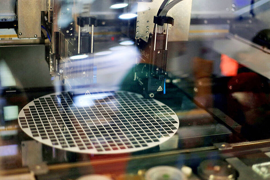
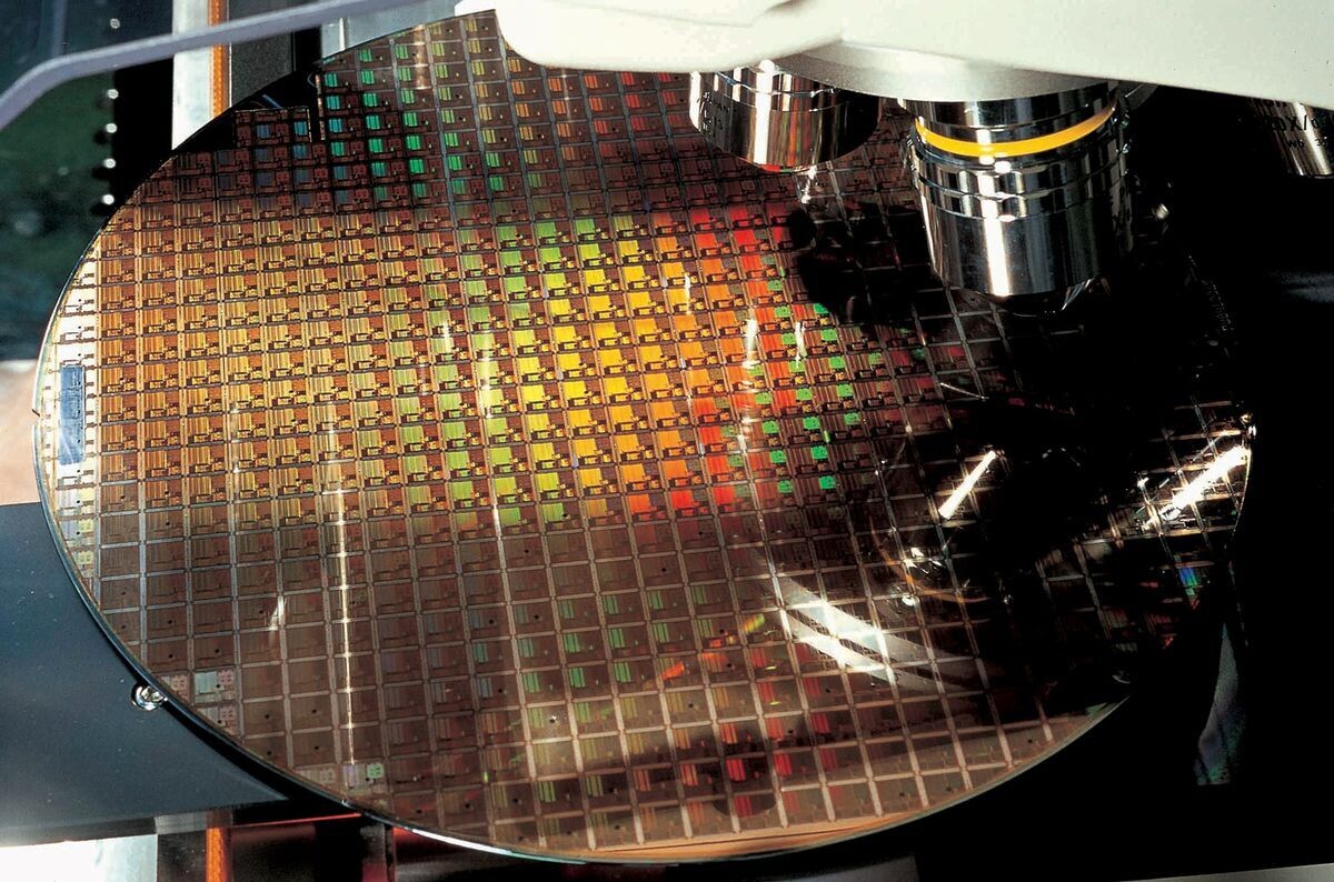
China is on course to become the world's leading semiconductor manufacturing hub by the end of the decade. Market research firm Yole Group predicts that by 2030, China will account for 30% of global foundry capacity, a sharp increase from its 21% share in 2024. This growth will position China ahead of Taiwan, which currently holds a 23% market share. In recent years, Beijing has committed vast public and private resources to domestic chip production. Last year, Chinese fabs processed 8.85 million wafers per month, marking an annual increase of approximately 15%. That output will rise to 10.1 million wafers per month in 2025. Much of this expansion comes from the commissioning of 18 new fabs. For example, Huahong Semiconductor opened its 12‑inch facility in Wuxi and began volume production in the first quarter of 2025.

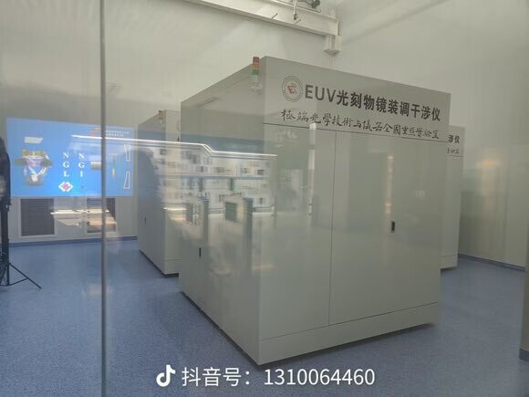
Despite strong capacity growth, China still faces significant issues. The United States is the world's largest wafer consumer, with 57% of global demand, yet it produces only about 10% of the total supply. As a result, American firms must import most of their chips from Asian foundries. Japan and Europe enjoy a more balanced situation by relying on domestic production to meet local needs. China's manufacturers also confront technological barriers. Export controls imposed by the United States limit their access to the most advanced lithography equipment and EDA software. To address this gap, Beijing has launched substantial initiatives to develop homegrown tools and software solutions. These efforts are crucial to closing the divide at cutting‑edge process nodes even as output volumes continue to grow. For now, China is emerging as the leader in mature node output, an area that the automotive sector is particularly interested in.

Rapidus Announces Collaboration with Siemens for 2 nm Semiconductor Design

Rapidus Corporation, a manufacturer of advanced logic semiconductors, today announced a strategic collaboration with Siemens Digital Industries Software for semiconductor design and manufacturing processes for the 2 nm generation. Rapidus will collaborate with Siemens to jointly develop a process design kit based on the Calibre platform, the industry-standard verification solution that enables highly accurate and efficient physical verification, manufacturing optimization and reliability assessment from semiconductor design through to fabrication, while continuing to further its design and verification ecosystem.

This collaboration supports the manufacturing for design (MFD) concept advocated by Rapidus to achieve high yield and short turnaround time from the early stages of manufacturing. Further, Rapidus and Siemens EDA will build a reference flow that holistically supports design, verification and manufacturing from front-end to back-end. This reference flow provides a smooth development environment for Rapidus' Rapid and Unified Manufacturing Service (RUMS).

Texas Instruments to Invest More Than $60 Billion Across Seven U.S. Semiconductor Fabs

Texas Instruments (TI) today announced its plans to invest more than $60 billion across seven U.S. semiconductor fabs, making this the largest investment in foundational semiconductor manufacturing in U.S. history. Working with the Trump administration and building on the company's nearly 100-year legacy, TI is expanding its U.S. manufacturing capacity to supply the growing need for semiconductors that will advance critical innovations from vehicles to smartphones to data centers. Combined, TI's new manufacturing mega-sites in Texas and Utah will support more than 60,000 U.S. jobs.

"TI is building dependable, low-cost 300 mm capacity at scale to deliver the analog and embedded processing chips that are vital for nearly every type of electronic system," said Haviv Ilan, president and CEO of Texas Instruments. "Leading U.S. companies such as Apple, Ford, Medtronic, NVIDIA and SpaceX rely on TI's world-class technology and manufacturing expertise, and we are honored to work alongside them and the U.S. government to unleash what's next in American innovation."

Micron and Trump Administration Announce Expanded U.S. Investments in Leading-Edge DRAM Manufacturing and R&D

Micron Technology, Inc. (Nasdaq: MU) and the Trump Administration today announced Micron's plans to expand its U.S. investments to approximately $150 billion in domestic memory manufacturing and $50 billion in R&D, creating an estimated 90,000 direct and indirect jobs. As part of today's announcement, Micron plans to invest an additional $30 billion beyond prior plans which includes building a second leading-edge memory fab in Boise, Idaho; expanding and modernizing its existing manufacturing facility in Manassas, Virginia; and bringing advanced packaging capabilities to the U.S. to enable long-term growth in High Bandwidth Memory (HBM), which is essential to the AI market. Additionally, Micron is announcing a planned $50 billion domestic R&D investment, reaffirming its long-term position as the global memory technology leader. As previously announced, Micron's investment includes its ongoing plans for a megafab in New York.

Micron's approximately $200 billion broader U.S. expansion vision includes two leading-edge high-volume fabs in Idaho, up to four leading-edge high-volume fabs in New York, the expansion and modernization of its existing manufacturing fab in Virginia, advanced HBM packaging capabilities and R&D to drive American innovation and technology leadership. These investments are designed to allow Micron to meet expected market demand, maintain share and support Micron's goal of producing 40% of its DRAM in the U.S. The co-location of these two Idaho fabs with Micron's Idaho R&D operations will drive economies of scale and faster time to market for leading-edge products, including HBM.

TSMC Can't Track Where Its Chips End Up, Annual Report Admits

TSMC has acknowledged fundamental visibility limitations in its semiconductor supply chain, stating in its latest annual report that it "inherently lacks visibility regarding the downstream use or user of final products." This disclosure relates to an incident where 7 nm chips manufactured for Sophgo were later identified in Huawei's Ascend 910B/C AI accelerators, whose hardware is subject to US export restrictions. The contract foundry outlined its standard process: receiving GDS files through intermediaries, validating technical specifications, creating photomasks, and fabricating wafers without insight into end applications. Subsequent analysis revealed that those very chips matched Huawei's specifications, providing components for approximately one million dual‑chiplet AI accelerator units, with two million dies shipped to Huawei.

The report warns that compliance violations by supply‑chain partners, such as failing to secure proper import, export or re‑export permits, could trigger regulatory investigations and penalties, even when TSMC adheres to its established protocols. US already proposed a $1 billion fine for TSMC. This visibility gap just shows that challenges in semiconductor manufacturing, where complex distribution networks obscure the path between fabrication and deployment, are not easily overcome. Foundries are facing increasing pressure to enhance tracking capabilities despite the inherent limitations of the contract manufacturing model. US sanctions on Chinese companies are growing their walls even higher, and this could mean that sanction-abiding companies might avoid doing business with Chinese entities altogether to avoid getting fined.

AMD Achieves First TSMC N2 Product Silicon Milestone

AMD today announced its next-generation AMD EPYC processor, codenamed "Venice," is the first HPC product in the industry to be taped out and brought up on the TSMC advanced 2 nm (N2) process technology. This highlights the strength of AMD and TSMC semiconductor manufacturing partnership to co-optimize new design architectures with leading-edge process technology. It also marks a major step forward in the execution of the AMD data center CPU roadmap, with "Venice" on track to launch next year. AMD also announced the successful bring up and validation of its 5th Gen AMD EPYC CPU products at TSMC's new fabrication facility in Arizona, underscoring its commitment to U.S. manufacturing.

"TSMC has been a key partner for many years and our deep collaboration with their R&D and manufacturing teams has enabled AMD to consistently deliver leadership products that push the limits of high-performance computing," said Dr. Lisa Su, chair and CEO, AMD. "Being a lead HPC customer for TSMC's N2 process and for TSMC Arizona Fab 21 are great examples of how we are working closely together to drive innovation and deliver the advanced technologies that will power the future of computing."

Tariffs Push US Wafer Fab Equipment Costs Up 15% for Domestic Fabs

As the US works to bring more semiconductor manufacturing back home, the machines needed to turn silicon into the world's most advanced processors are becoming pricier and harder to get, thanks to tariffs. Foundries building new fabs report that the specialized equipment they rely on, everything from extreme ultraviolet (EUV) lithography steppers to chemical vapor deposition chambers, carries a roughly 15% premium compared with similar gear sold overseas. Several forces are at play. The raw materials, high‑grade quartz for vacuum enclosures, and exotic metal alloys for precision optics have climbed in price. At the same time, key components like ultra‑accurate motion stages and alignment sensors are in short supply, sometimes stretching lead times for critical subsystems well beyond 18 months. For a fab racing to move from a 7 nm to a 5 nm process, those delays can mean missing tight ramp‑up targets and pushing out product launches.

Smaller chipmakers feel the squeeze the hardest. With fewer orders to negotiate volume discounts, second‑tier foundries may see their capital budgets balloon by 20 percent or more. In response, some are taking a mixed approach, sourcing commoditized tools such as oxidation furnaces and rapid thermal processors from multiple suppliers while reserving single‑vendor deals for high‑stakes systems like EUV scanners. Government support through the CHIPS Act offers a partial safety net, helping to subsidize capital expenditures. Yet even with grants and tax credits, the challenges will remain. Success will hinge on tight coordination between fabs, equipment makers, and policymakers to tame rising costs, shorten delivery schedules, and keep America's chip renaissance on track.

Intel and TSMC in Foundry Joint Venture Talks

Intel and TSMC are reportedly locked in talks to form a semiconductor foundry joint-venture (JV). This sensational piece of news comes from Reuters, which says that the two companies have reached a preliminary agreement to form the JV. Apparently, the move saves TSMC from building any hard infrastructure on U.S. soil, and instead use Intel's semiconductor foundry facilities. This would hence bring TSMC's semiconductor manufacturing IP and workforce to the U.S., however it remains to be seen if the very latest foundry technology would be handed over to the JV. TSMC would hold a 20% stake in the venture, and Intel the rest. Investors of Intel and TSMC reacted very differently to the news, with the TSMC stock falling 6% and Intel gaining 5%. Reuters also reports that it was the Trump Administration that negotiated this joint-venture between TSMC and Intel in a bid to "revitalize Intel."

US Exempts Semiconductors From Taiwan Tariffs, But Chip-Making Equipment Remains on the List

Yesterday, United States President Donald Trump announced a set of tariffs imposed on US trading partners, imposing a series of 10%+ tariffs on partners, calling it a "Liberation Day." Today, we are calculating how much these tariffs will impact consumers and what is most important at TechPowerUp: semiconductors powering our GPUs and CPUs. According to one of the top investment banks, Goldman Sachs, semiconductors are exempt from the reciprocal tariffs that Trump has imposed on Taiwan. However, the semiconductor manufacturing equipment used by makers like TSMC is not exempt and is expected to be hit with the 32% tariffs. This is only half of what Taiwan imposes on imports of US-made goods. For TSMC, the number one maker of GPUs and CPUs, tariffs can be tricky to navigate. While its existing manufacturing facilities use equipment sourced from Dutch ASML and a few US companies like Lam Research and KLA Corporation, it shouldn't be a problem to ship new silicon to the US.

However, if TSMC wants to expand its manufacturing facilities in any country that is not the US, it will have to deal with 32% tariffs on US-sourced silicon manufacturing equipment. For EU-based ASML, things are looking a little different. If over 20% of the equipment is made up of US content, a tariff exemption might apply, potentially reducing import costs. If more than one-fifth of a product's components or value originates from US sources, the equipment may be eligible for tariff relief. ASML's machines include some US components, so determining whether these machines meet the 20% threshold is crucial. If they do, the tariff exemption could help lower costs associated with importing these advanced machines, reaching up to $380 million. For non-US-injected goods, EU entities are subject to 20% tariffs.

TSMC Reportedly Preparing New Equipment for 1.4 nm Trial Run at "P2" Baoshan Plant

Industry insiders posit that TSMC's two flagship fabrication facilities are running ahead of schedule with the development of an advanced 2 nm (N2) process node. A cross-facility mass production phase is tipped to begin later this year, which leaves room for next-level experiments. Taiwan's Economic Daily News has heard supply chain whispers about the Baoshan "P2" plant making internal preparations for a truly cutting edge 1.4 nm-class product. According to the report, unnamed sources have claimed that: "TSMC has made a major breakthrough in the advancement of its 1.4 nm process. (The company) has recently notified suppliers to prepare the necessary equipment for 1.4 nm, and plans to install a trial production 'mini-line' at P2 (Baoshan Fab 20)."

Their Hsinchu-adjacent "Fab 20" site is touted as a leading player in the prototyping of this new technology. Industry moles reckon that "1.4 nm expertise" will eventually trickle over to nearby "P3 and P4 plants" for full production phases. Allegedly, these factories were originally going to be involved in the manufacturing of 2 nm (N2) wafers. Additionally, TSMC's "Fab 25" campus could potentially play host to trial 1.4 nm activities—the Economic Daily News article proposes that four plants based in the Central Taiwan Science Park are pitching in with collaborative work. As interpreted by TrendForce, "P1" could begin "risk trial production" by 2027, followed by full-scale output within the following year.

Rapidus Confirms Launching 2nm Pilot Line in April, Mass Production Set for 2027

Rapidus Corporation today announced that its plans and budget for fiscal year 2025 have been approved by Japan's New Energy and Industrial Technology Development Organization (NEDO). The approval covers two commissioned projects under NEDO's "Post-5G Information and Communication Systems Infrastructure Enhancement R&D Project / Development of Advanced Semiconductor Manufacturing Technology (Commissioned)." These projects are the "Research and Development of 2 nm-Generation Semiconductor Integration Technology and short TAT (turnaround time) Manufacturing Technology Based on Japan-U.S. Collaboration" and "Development of Chiplet, Package Design and Manufacturing Technology for 2 nm-Generation Semiconductors."

The first of these projects, focused on front-end processes, was launched in November 2022 as part of Japan's next-generation semiconductor R&D effort. Under this program, Rapidus has continued construction of the Innovative Integration for Manufacturing (IIM) facility in Chitose, Hokkaido, which will serve as its production base. It also sent engineers to IBM in the U.S. to jointly develop 2 nm logic semiconductor mass production technologies and continued to achieve target performance as planned. Furthermore, Rapidus has installed EUV lithography and other production equipment at the IIM facility, and started cleanroom operation. As a result of these efforts, the company achieved its performance targets for FY2024.

Russia Unveils Domestic 350 nm Lithography System Amid Sanctions

Russian and Belarusian semiconductor manufacturers have achieved a significant milestone in domestic chip production capabilities. In collaboration with Belarus-based Planar, the Zelenograd Nanotechnology Center (ZNTC) has developed a new lithography system supporting 350 nm process technology for 8-inch (200 mm) silicon wafers. This development represents a strategic response to Western sanctions severely restricting Russia's access to advanced semiconductor manufacturing equipment. The system employs solid-state laser technology to project circuit patterns onto photoresist-coated wafers through a photomask that defines the circuitry. After selective exposure, the photoresist undergoes chemical processing to build circuit structures. While the 350 nm node marks a critical capability for domestic semiconductor production, it sits almost three decades behind leading-edge fabrication processes in high-performance computing applications.

This technology is comparable to what powered Intel's Pentium II processors in the late 1990s. Despite this technological gap, the equipment will enable the production of various electronic components suitable for consumer electronics and certain specialized military applications where bleeding-edge performance isn't required. ZNTC has already outlined plans to develop a more advanced 130 nm lithography system by 2026 as part of a government-backed initiative to incrementally enhance domestic semiconductor capabilities. While unable to match the 3-5 nm processes currently deployed by global semiconductor leaders, this lithography system establishes a foundation for domestic chip manufacturing infrastructure, especially in the category of mature nodes. The success of this intermediate solution will likely influence government funding priorities as the country attempts to narrow the technological gap with Western semiconductor capabilities in the coming years.

Intel to Receive $1.9 Billion as SK Hynix Finalizes NAND Deal

Intel and SK Hynix have finalized an $8.85 billion transaction involving Intel's NAND flash memory operations, marking the conclusion of a two-phase deal initiated in 2020. In the first phase of the transaction, SK Hynix acquired Intel's SSD division along with a NAND production facility in Dalian, China, for $6.61 billion. The Dalian facility was later rebranded as Solidigm. Notably, this phase transferred only the physical assets and operational facilities, leaving behind critical intellectual property, research and development infrastructure, and specialized technical staff. The second phase, finalized with a payment of $1.9 billion this Tuesday, addressed these remaining components. With this payment, SK Hynix secured full rights to Intel's proprietary NAND technology, R&D resources, and the technical workforce dedicated to NAND operations.

During the transition period, Intel maintained control over these elements, which limited integration between Solidigm and Intel's NAND teams. This separation was designed to manage operational risks and gradually transfer capabilities. Completing this deal helps with a strategic restructuring of Intel's portfolio as it shifts focus toward high-growth areas such as AI chip development, foundry services, and next-generation semiconductor manufacturing. A $1.9 billion financial injection is perfect in time for Intel Foundry business, burning billions per year, to offset some of the losses. For SK Hynix, consolidating the complete range of Intel's NAND operations enhances its competitive position in the global NAND market, providing access to established technologies and key industry expertise. This finalization is part of a broader trend where companies divest from commoditized memory products to concentrate on more advanced semiconductor solutions like AI chips and other accelerators, which are enjoying higher margins and a better business outlook.

YES Pioneers Semiconductor Equipment Production in India

Yield Engineering Systems, Inc. (YES), a global leader in materials and interface engineering equipment solutions, proudly announces the shipment of the first commercial VeroTherm Formic Acid Reflow tool to a leading global semiconductor manufacturer from its Sulur, Coimbatore, manufacturing facility. This landmark achievement signifies a pivotal moment for YES and the burgeoning semiconductor ecosystem in India, as it represents the first equipment produced in India for advanced semiconductor applications like High Bandwidth Memory (HBM), which is critical for AI and High-Performance Computing (HPC) applications worldwide.

YES commenced operations in September 2024 at this state-of-the-art manufacturing facility in Sulur, Coimbatore, India, located at 96/3 Vadakku Sambala Thottam, Trichy Road, Kannampalayam, Sulur Taluk. This facility is integral to YES's strategic expansion plan, aimed at serving its global customers' operations in India and the world with greater efficiency.

Chinese SiCarrier Shows a Complete Silicon Manufacturing Flow: Deposition, Etching, Metrology, Inspection, and Electrical Testing

SiCarrier, a Huawei-backed Chinese semiconductor tool manufacturer, has launched a comprehensive suite of semiconductor manufacturing tools at this year's Semicon China. These tools are strategically essential to China's semiconductor self-sufficiency and a major step towards competitive nodes from the mainland. The new lineup spans multiple categories: optical inspection, deposition, etch, metrology, and electrical performance testing. Until now, Chinese chipmakers often depended on older-generation foreign equipment, but SiCarrier's new lineup promises domestic alternatives tailored to modern manufacturing processes. The tools address every stage of semiconductor fabrication, from inspecting microscopic defects to etching intricate circuits.

For quality control, SiCarrier's Color Mountain series functions like a high-powered microscope, using intense lighting and advanced imaging algorithms to examine both sides of silicon wafers for flaws as small as dust particles. Complementing this, the Sky Mountain series ensures the perfect alignment of circuit layers, which need perfect stacking, using diffraction-based measurements (analyzing light patterns) and direct image comparisons. The New Mountain suite combines specialized tools to analyze materials at the atomic level. One standout is the atomic force microscope (AFM), which maps surface topography with a nanoscale "finger," while X-ray techniques (XPS, XRD, XRF) act like forensic tools, revealing the chemical composition, crystal structure, and elemental makeup.

TSMC Arizona Operations Only 10% More Expensive Than Taiwanese Fab Operations

A recent study by TechInsights is reshaping the narrative around the cost of semiconductor manufacturing in the United States. According to the survey, processing a 300 mm wafer at TSMC's Fab 21 in Phoenix, Arizona, is only about 10% more expensive than similar operations in Taiwan. This insight challenges earlier assumptions based on TSMC founder Morris Chang's comments, which suggested that high fab-building expenses in Arizona made US chip production financially impractical. G. Dan Hutcheson of TechInsights highlighted that the observed cost difference largely reflects the expenses associated with establishing a brand-new facility. "It costs TSMC less than 10% more to process a 300 mm wafer in Arizona than the same wafer made in Taiwan," he explained. The initial higher costs stem from constructing a fab in an unfamiliar market with a new, sometimes unskilled workforce—a scenario not typical for mature manufacturing sites.

A significant portion of the wafer production cost is driven by equipment, which accounts for well over two-thirds of the total expenses. Leading equipment providers like ASML, Applied Materials, and Lam Research charge similar prices globally, effectively neutralizing geographic disparities. Although US labor costs are higher than in Taiwan, the heavy automation in modern fabs means that labor represents less than 2% of the overall cost. Additional logistics for Fab 21, including the return of wafers to Taiwan for dicing, testing, and packaging, add complexity but only minimally affect the overall expense. With plans to expand domestic packaging capabilities, TSMC's approach is proving to be strategically sound. This fresh perspective suggests that the apparent high cost of US fab construction has been exaggerated. TSMC's $100B investment in American semiconductor manufacturing reflects a calculated decision informed by detailed cost analysis—demonstrating that location-based differences become less significant when the equipment dominates expenses.

Vietnam to Begin First Wafer Fab Construction, Eyes Semiconductor Leadership in the Coming Decade

Vietnam's government has approved its first wafer fab facility, with an investment of 12.8 trillion VND (approximately $500 million). The first phase of the facility, scheduled for completion by 2030, is designed to manufacture specialized chips for defense, AI, and other high-tech applications. The project will receive government backing through direct funding—covering up to 30% of the total investment, capped at 10 trillion VND—and tax incentives. A special steering committee headed by the Prime Minister has been tasked with overseeing the project's execution and resource allocation. The new fab is a critical component of Vietnam's long-term semiconductor strategy, a phased approach toward building a domestic ecosystem for chip design, manufacturing, and testing. The current investment is modest compared to the typical costs of advanced wafer fabs, which can reach up to $50 billion.

Nonetheless, the project is a foundational, one-step-at-the-time move intended to spur further investments and technology transfer. Vietnamese officials have reportedly engaged in discussions with major international chip manufacturers—including US, South Korea, and Taiwan entities, such as GlobalFoundries and Powerchip Semiconductor Manufacturing Corp—to explore potential collaborative opportunities. Vietnam already hosts 174 semiconductor-related projects, predominantly focused on chip packaging and testing, in which global companies like Intel and Amkor have established significant operations. The second phase, from 2030-2040, envisions Vietnam emerging as a worldwide center for electronics and semiconductors. By expanding to at least 200 design companies, establishing two semiconductor chip manufacturing plants, and creating 15 packaging and testing facilities, the country intends to gradually develop independent semiconductor product design and production capabilities.

Global Top 10 IC Design Houses See 49% YoY Growth in 2024, NVIDIA Commands Half the Market

TrendForce reveals that the combined revenue of the world's top 10 IC design houses reached approximately US$249.8 billion in 2024, marking a 49% YoY increase. The booming AI industry has fueled growth across the semiconductor sector, with NVIDIA leading the charge, posting an astonishing 125% revenue growth, widening its lead over competitors, and solidifying its dominance in the IC industry.

Looking ahead to 2025, advancements in semiconductor manufacturing will further enhance AI computing power, with LLMs continuing to emerge. Open-source models like DeepSeek could lower AI adoption costs, accelerating AI penetration from servers to personal devices. This shift positions edge AI devices as the next major growth driver for the semiconductor industry.

TSMC Still Continues to Explore Joint Venture for Intel Foundry Ownership

TSMC is still considering a strategic joint venture to operate Intel's manufacturing capacity, according to four sources close to Reuters that are familiar with the discussions. The proposed arrangement would limit TSMC's ownership to less than 50% and potentially distribute stakes to major American chip designers, including AMD, Broadcom, NVIDIA, and Qualcomm. The initiative emerged following direct intervention from the Trump administration, which has prioritized revitalizing domestic semiconductor manufacturing while maintaining American control of critical technology infrastructure. Under the proposed framework, Intel would spin off its Intel Foundry division, with TSMC acquiring a minority stake and bringing in partner companies as co-investors.

Apple, TSMC's largest customer, is absent from these preliminary discussions, suggesting careful strategic positioning within the competitive ecosystem—however, significant technical and operational challenges are facing the potential joint venture. Intel's manufacturing and real estate assets are valued at approximately $108 billion, requiring substantial capital commitments from prospective partners. More fundamentally, the technological integration presents massive obstacles, as Intel and TSMC utilize fundamentally different manufacturing processes with distinct equipment configurations and material requirements. However, the complex negotiations remain in the early stages, with significant technical, financial, and regulatory hurdles to overcome before any formal agreement materializes. Intel is still not giving the clear green light to spin off rumors.

China Develops Domestic EUV Tool, ASML Monopoly in Trouble

China's domestic extreme ultraviolet (EUV) lithography development is far from a distant dream. The newest system, now undergoing testing at Huawei's Dongguan facility, leverages laser-induced discharge plasma (LDP) technology, representing a potentially disruptive approach to EUV light generation. The system is scheduled for trial production in Q3 2025, with mass manufacturing targeted for 2026, potentially positioning China to break ASML's technical monopoly in advanced lithography. The LDP approach employed in the Chinese system generates 13.5 nm EUV radiation by vaporizing tin between electrodes and converting it to plasma via high-voltage discharge, where electron-ion collisions produce the required wavelength. This methodology offers several technical advantages over ASML's laser-produced plasma (LPP) technique, including simplified architecture, reduced footprint, improved energy efficiency, and potentially lower production costs.

The LPP method relies on high-energy lasers and complex FPGA-based real-time control electronics to achieve the same result. While ASML has refined its LPP-based systems over decades, the inherent efficiency advantages of the LDP approach could accelerate China's catch-up timeline in this critical semiconductor manufacturing technology. When the US imposed sanctions on EUV shipments to Chinese companies, the Chinese semiconductor development was basically limited as standard deep ultraviolet (DUV) wave lithography systems utilize 248 nm (KrF) and 193 nm (ArF) wavelengths for semiconductor patterning, with 193 nm immersion technology representing the most advanced pre-EUV production technique. These longer wavelengths contrast with EUV's 13.5 nm radiation, requiring multiple patterning techniques to achieve advanced nodes.

Intel Confirms Long-Term TSMC Partnership, About 30% of Wafers Outsourced to TSMC

Intel still depends on external partners for its semiconductor manufacturing strategy, with approximately 30% of its wafers currently outsourced to TSMC, according to Intel's Corporate Vice President of Investor Relations. This marks a significant shift from previous plans to eliminate external foundry dependencies, as the company now intends to maintain a permanent multi-foundry approach. "That is probably a high watermark for us," said John Pitzer during a recent investor dialogue with Morgan Stanley analyst Joe Moore. "But to the extent that I think a year ago, we were talking about trying to get that to zero as quickly as possible. That's no longer the strategy." Pitzer elaborated that Intel now views TSMC as "a great supplier" whose continued involvement "creates a good competition between them and Intel Foundry." The company is reportedly evaluating the optimal long-term outsourcing ratio, considering targets between 15-20% of total wafer production.

This strategic adjustment comes amid leadership changes at Intel, with interim CEOs Dave Zinsner and Michelle Johnston Holthaus granted increased decision-making authority while maintaining the core dual approach of developing "a world-class fabless company and a world-class foundry." The executive team focuses on strengthening Intel's product competitiveness before fully optimizing its foundry operations. This pragmatic approach is viewed as recognizing manufacturing realities in the highly complex semiconductor creation. Intel's willingness to leverage TSMC's advanced process technologies reflects both practical necessity and strategic flexibility as the company navigates its manufacturing transformation. Intel's fabrication self-sufficiency goals remain essential but will be balanced against product competitiveness and time-to-market considerations.

Intel Products Unveils Assured Supply Chain Program for Enterprises

Intel Products today launched the Intel Assured Supply Chain (ASC) program, designed to provide additional transparency and assurance in the silicon manufacturing process. This specialized client system-on-chip (SoC) solution, initially offered on specific Intel Core Ultra Series 2 mobile and desktop SKUs, provides a digitally
attestable chain of custody of each chip's progress through the chip manufacturing process, leveraging a dedicated chip manufacturing pathway through specific Intel
manufacturing locations. With the ASC program, Intel Products delivers added transparency into processor manufacturing, assuring customers about the locations of
their silicon supply chain.

"Intel has long been a leader in secure, transparent and reliable semiconductor manufacturing, and the Intel Assured Supply Chain program is another step forward in strengthening trust in the technology that powers our customers' critical operations," said Jennifer Larson, general manager, Commercial Client Segments, Client Computing Group, Intel.

TSMC Intends to Expand Its Investment in the United States to US$165 Billion to Power the Future of AI

TSMC (TWSE: 2330, NYSE: TSM) today announced its intention to expand its investment in advanced semiconductor manufacturing in the United States by an additional $100 billion. Building on the company's ongoing $65 billion investment in its advanced semiconductor manufacturing operations in Phoenix, Arizona, TSMC's total investment in the U.S. is expected to reach US$165 billion. The expansion includes plans for three new fabrication plants, two advanced packaging facilities and a major R&D team center, solidifying this project as the largest single foreign direct investment in U.S. history.

Through this expansion, TSMC expects to create hundreds of billions of dollars in semiconductor value for AI and other cutting-edge applications. TSMC's expanded investment is expected to support 40,000 construction jobs over the next four years and create tens of thousands of high-paying, high-tech jobs in advanced chip manufacturing and R&D. It is also expected to drive more than $200 billion of indirect economic output in Arizona and across the United States in the next decade. This move underscores TSMC's dedication to supporting its customers, including America's leading AI and technology innovation companies such as Apple, NVIDIA, AMD, Broadcom, and Qualcomm.

Intel Announces Ohio One Construction Timeline Update

On Feb. 28, 2025, Naga Chandrasekaran, executive vice president, chief global operations officer and general manager of Intel Foundry Manufacturing, sent a message to Intel employees in Ohio updating them on the latest planned construction completion dates for Ohio One Mod 1 and Mod 2 that are under construction in New Albany, Licking County, Ohio. I continue to be impressed by the progress you are driving on our Ohio One campus. We have come a long way since construction began, and I am grateful for all that you've accomplished to lay the groundwork for our future as we make Ohio one of the world's leading hubs of advanced semiconductor manufacturing.

Last quarter, we achieved our "go vertical" milestone when the "basement" level of the fab was completed - and work on the above-ground structure is now underway. The campus has been transformed in ways that bring Ohio's natural beauty to the site. You are also doing so much beyond our campus to support Ohioans in our neighborhood and across the state by creating education and workforce development initiatives, building local business partnerships, and volunteering and investing in the community. I am proud of the impact you are making.

Intel 18A Node SRAM Density On-Par with TSMC, Backside Power Delivery a Big Bonus

Intel has unveiled some interesting advances in semiconductor manufacturing at the International Solid-State Circuits Conference (ISSCC), showcasing the capabilities of its highly anticipated Intel 18A process technology. The presentation highlighted significant improvements in SRAM bit cell density. The PowerVia system, coupled with RibbonFET (GAA) transistors, is at the heart of Intel's node. The company demonstrated solid progress with their high-performance SRAM cells, achieving a reduction from 0.03 µm² in Intel 3 to 0.023 µm² in Intel 18A. High-density cells showed similar improvement, shrinking to 0.021 µm². These advancements represent scaling factors of 0.77 and 0.88 respectively, which are significant achievements in SRAM technology, once thought to be done with scaling benefits.

Implementing PowerVia technology is an Intel-first approach to addressing voltage drops and interference in processor logic areas. Using an "around the array" scheme, Intel strategically applies PowerVias to I/O, control, and decoder elements while optimizing bit cell design without a frontal power supply. The macro bit density of 38.1 MBit/mm² achieved by Intel 18A puts the company in a strong competitive position. While TSMC reported matching figures with their N2 process, Intel's comprehensive approach with 18A, combining PowerVia and GAA transistors, could challenge Smausng and TSMC, with long-term aspirations to compete for premium clients currently served by TSMC, including giants like NVIDIA, Apple, and AMD.
Return to Keyword Browsing
Jul 5th, 2025 23:22 CDT change timezone

New Forum Posts

Popular Reviews

TPU on YouTube

Controversial News Posts