News Posts matching #semiconductor manufacturing

Return to Keyword Browsing

Intel Introduces First-of-its-Kind Semiconductor Co-Investment Program

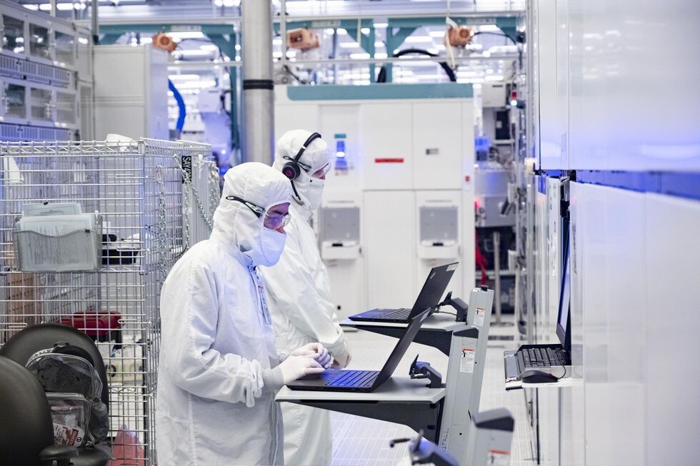
Intel Corporation today announced a first-of-its-kind Semiconductor Co-Investment Program (SCIP) that introduces a new funding model to the capital-intensive semiconductor industry. As part of its program, Intel has signed a definitive agreement with the infrastructure affiliate of Brookfield Asset Management, one of the largest global alternative asset managers, which will provide Intel with a new, expanded pool of capital for manufacturing build-outs.

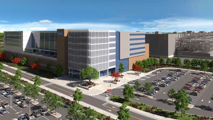
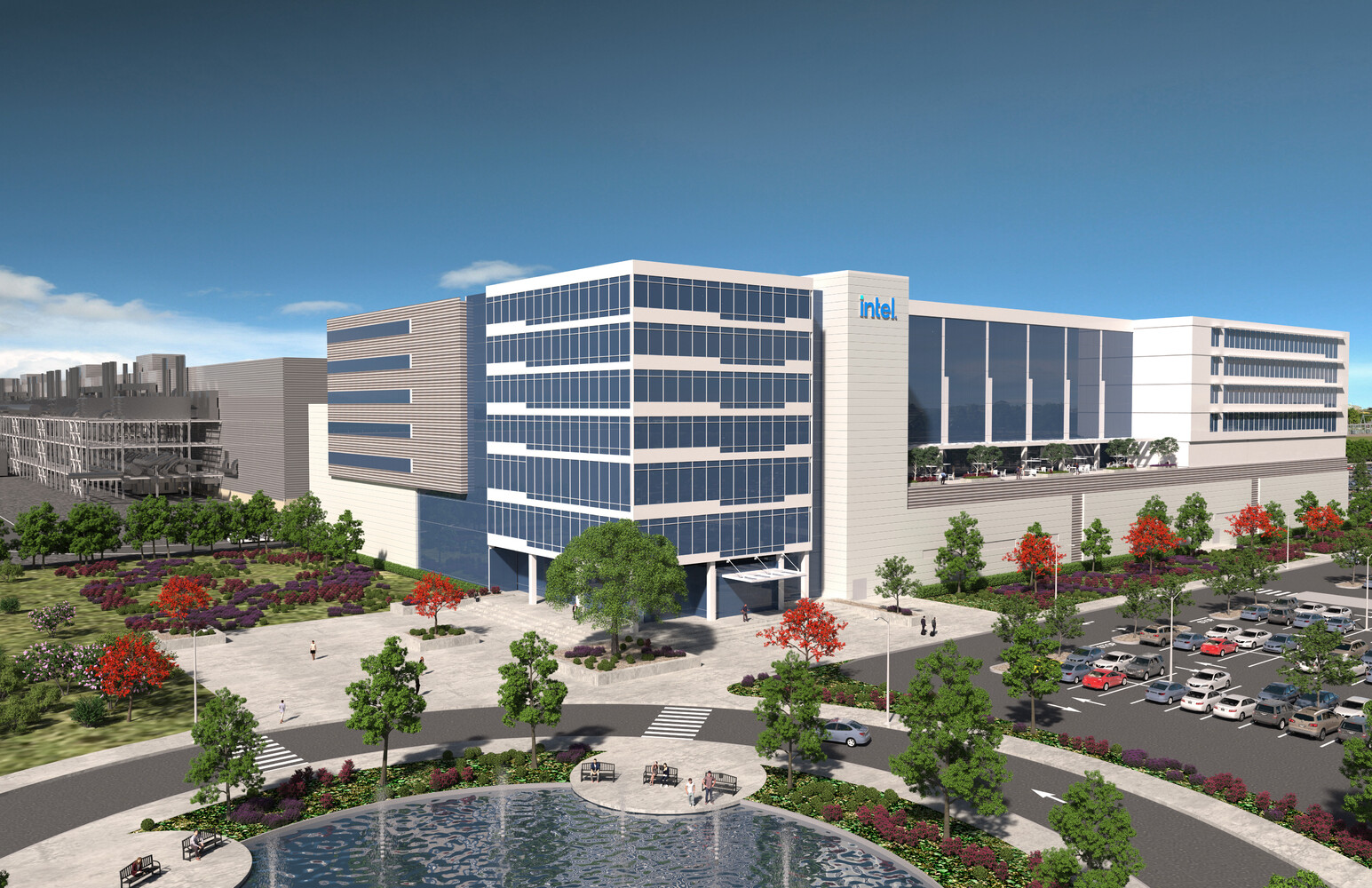
SCIP is a key element of Intel's Smart Capital approach, which aims to provide innovative ways to fund growth while creating further financial flexibility to accelerate the company's IDM 2.0 strategy. Intel's agreement with Brookfield follows the two companies' memorandum of understanding announced in February 2022. Under the terms of the agreement, the companies will jointly invest up to $30 billion in Intel's previously announced manufacturing expansion at its Ocotillo campus in Chandler, Arizona, with Intel funding 51% and Brookfield funding 49% of the total project cost. Intel will retain majority ownership and operating control of the two new leading-edge chip factories in Chandler, which will support long-term demand for Intel's products and provide capacity for Intel Foundry Services (IFS) customers. The transaction with Brookfield is expected to close by the end of 2022, subject to customary closing conditions.

US President Biden Signs Off on the CHIPS and Science Act

In President Biden's first year in office, the Biden-Harris Administration has implemented an industrial strategy to revitalize domestic manufacturing, create good-paying American jobs, strengthen American supply chains, and accelerate the industries of the future. These policies have spurred an historic recovery in manufacturing, adding 642,000 manufacturing jobs since 2021. Companies are investing in America again, bringing good-paying manufacturing jobs back home. The construction of new manufacturing facilities has increased 116 percent over last year.

Today, President Biden will sign into law the bipartisan CHIPS and Science Act of 2022, which will build on this progress, making historic investments that will poise U.S. workers, communities, and businesses to win the race for the 21st century. It will strengthen American manufacturing, supply chains, and national security, and invest in research and development, science and technology, and the workforce of the future to keep the United States the leader in the industries of tomorrow, including nanotechnology, clean energy, quantum computing, and artificial intelligence. The CHIPs and Science Act makes the smart investments so that American to compete in and win the future.

GlobalFoundries and Qualcomm Announce Extension of Long-term Agreement to Secure U.S. Supply through 2028

Following the recent passage of the U.S. CHIPS and Science Act last week, GlobalFoundries (Nasdaq: GFS) (GF), a global leader in feature-rich semiconductor manufacturing and Qualcomm Technologies, Inc. today announced they are more than doubling their existing strategic global long-term semiconductor manufacturing agreement previously entered into by GF's and Qualcomm's respective subsidiaries. Today's announcement secures wafer supply and commitments to support U.S.-based manufacturing through capacity expansion at GF's most advanced semiconductor manufacturing facility, in Malta, New York.

The announcement was made in Washington D.C. at a CEO Summit co-hosted by GF, Ford Motor Company, and Applied Materials, which included National Economic Council Director Brian Deese, Under Secretary of Defense for Acquisition & Sustainability Dr. William LaPlante, and National Security Council Senior Director for Technology & National Security, Tarun Chhabra underscoring the importance of domestic manufacturing to national and economic security. The Summit included CEOs and senior leaders from across the semiconductor supply chain from tool and wafer manufacturers to key suppliers to end users of chips manufactured in the U.S.

Micron Announces Intent to Bring Leading-Edge Memory Manufacturing to the U.S.

Micron Technology, Inc. (NASDAQ: MU) commends and thanks the Biden Administration for their leadership and the bipartisan work of Congress for passing the "Chips and Science" legislation. This is a big step towards securing the future of semiconductor manufacturing in the United States and advancing American innovation and competitiveness for years to come.

This legislation will bring leading-edge semiconductor manufacturing to the U.S., creating tens of thousands of jobs and tens of billions of dollars of new investments - transforming U.S. semiconductor innovation and supply chain resilience.

Intel and MediaTek Form Foundry Partnership

Intel and MediaTek today announced a strategic partnership to manufacture chips using Intel Foundry Services' (IFS) advanced process technologies. The agreement is designed to help MediaTek build a more balanced, resilient supply chain through the addition of a new foundry partner with significant capacity in the United States and Europe. MediaTek plans to use Intel process technologies to manufacture multiple chips for a range of smart edge devices. IFS offers a broad manufacturing platform with technologies optimized for high performance, low power and always-on connectivity built on a roadmap that spans production-proven three-dimensional FinFET transistors to next-generation breakthroughs.

"As one of the world's leading fabless chip designers powering more than 2 billion devices a year, MediaTek is a terrific partner for IFS as we enter our next phase of growth," said IFS President Randhir Thakur. "We have the right combination of advanced process technology and geographically diverse capacity to help MediaTek deliver the next billion connected devices across a range of applications."

Chinese SMIC Ships 7 nm Chips, Reportedly Copied TSMC's Design

The Chinese technology giant, SMIC, has managed to advance its semiconductor manufacturing technology and shipped the first 7 nm silicon manufactured on China's soil. According to analyst firm TechInsights, who examined the 7 nm Bitcoin mining SoC made for MinerVa firm, there are doubts that SMIC 7 nm process is somewhat similar to TSMC's 7 nm process. Despite having no access to advanced semiconductor manufacturing tools, and US restrictions placed around it, SMIC has managed to produce what resembles an almost perfect 7 nm node. This could lead to a true 7 nm logic and memory bitcells sometimes in the future, as the node advances in SMIC's labs.

Having done an in-depth die analysis, the TechInsights report indicates that TSMC, Intel, and Samsung have a more advanced 7 nm node and are two nodes ahead of the Chinese SMIC. The results are not great regarding the economics and yield of this SMIC 7 nm process. While we have no specific data, the report indicates that the actual working chips made with older DUV tools are not perfect. This is not a problem for the Chinese market as it seeks independence from Western companies and technology. However, introducing a China-made 7 nm chip is more critical as it shows that the country can manufacture advanced nodes with restrictions and sanctions in place. The MinerVa SoC die and the PCB that houses those chips are pictured below.

Microsoft Azure Joins Intel Foundry Services Cloud Alliance

The recent semiconductor shortage has put an unprecedented amount of focus on the industry. Both commercial and government entities have come to recognize the lack of advanced node semiconductor manufacturing capabilities onshore in the United States. Intel Foundry Services (IFS) entry into the commercial foundry space is poised to change all that. As part of IFS Accelerator program, Intel recently announced their new IFS Cloud Alliance program, with Microsoft Azure as one of the inaugural members.

This is the latest chapter in a partnership between Intel and Microsoft that stretches back decades all the way back to the early days of the personal computer. In the last few years, Intel and Microsoft have collaborated on advancing semiconductor design on the cloud by working together to bring out EDA centric cloud compute such as the FX series on Azure, working with EDA vendors to enhance their software to better take advantage of the elasticity of the Azure cloud, as well as collaborating on a secure cloud-based semiconductor development platform for the US Department of Defense RAMP and RAMP-C programs.

STMicroelectronics and GlobalFoundries to advance FD-SOI ecosystem with new 300mm manufacturing facility in France

STMicroelectronics, a global semiconductor leader serving customers across the spectrum of electronics applications, and GlobalFoundries Inc., a global leader in feature-rich semiconductor manufacturing, today announced they have signed a Memorandum of Understanding to create a new, jointly-operated 300 mm semiconductor manufacturing facility adjacent to ST's existing 300 mm facility in Crolles, France. This facility is targeted to ramp at full capacity by 2026, with up to 620,000 300 mm wafer per year production at full build-out (~42% ST and ~58% GF).

ST and GF are committed to building capacity for their European and global customer base. This new facility will support several technologies, in particular FD-SOI-based technologies, and will cover multiple variants. This includes GF's market leading FDX technology and ST's comprehensive technology roadmap down to 18 nm, which are expected to remain in high demand for Automotive, IoT, and Mobile applications for the next few decades. FD-SOI technology has origins in the Grenoble (France) area. It has been part of ST technology and product roadmap in its Crolles facility since the early beginnings, and it was later enabled with differentiation and commercialized for manufacturing at GF's Dresden facility. FD-SOI offers substantial benefits for designers and customers, including ultra-low power consumption as well as easier integration of additional features such as RF connectivity, mmWave and security.

Japan and the US Joins Forces to Produce 2 nm Chips in Japan by 2025

Based on a report by the Nikkei, Japan and the US have joined forces to speed up the development of semiconductor production at 2 nm nodes in Japan by 2025. It's not exactly clear how this is going to happen, but the two nations are said to have signed a bilateral chip technology partnership. The heavy lifting is said to be done by private companies from both nations, but in terms of research and actual chip production. Part of the reason for the move, is that Japan wants to be able to manufacture cutting edge ICs domestically for next-generation chips.

The research is said to be kicking off as soon as this summer, although no decisions have been made with regards to the manufacturing structure, with the Nikkei suggesting two alternatives, based on information from the Japanese Ministry of Economy. There will either be a joint partnership between Japanese and US businesses, or it could be a wholly Japanese owned setup. It appears that one major reason for this project is the production of ICs for the Japanese defence industry, as advanced electronics are needed in a lot of related products, ranging from fighter jets and missiles, to radar systems and communication systems. However, the article also suggests that the 2 nm node is suitable for everything from components for quantum computers to smartphones. Japan already makes advanced silicon wafers and many other parts and components used in semiconductor manufacturing, but the nation has fallen behind in the actual manufacturing of leading edge semiconductors over the past few years.

Intel 4 Process Node Detailed, Doubling Density with 20% Higher Performance

Intel's semiconductors nodes have been quite controversial with the arrival of the 10 nm design. Years in the making, the node got delayed multiple times, and only recently did the general public get the first 10 nm chips. Today, at IEEE's annual VLSI Symposium, we get more details about Intel's upcoming nodes, called Intel 4. Previously referred to as a 7 nm process, Intel 4 is the company's first node to use EUV lithography accompanied by various technologies. The first thing when a new process node is discussed is density. Compared to Intel 7, Intel 4 will double the transistor count for the same area and enable 20% higher performing transistors.

Looking at individual transistor size, the new Intel 4 node represents a very tiny piece of silicon that is even smaller than its predecessor. With a Fin Pitch of 30 nm, Contact Gate Poly Pitch of 50 nm between gates, and Minimum Metal Pitch (M0) of 50 nm, the Intel 4 transistor is significantly smaller compared to the Intel 7 cell, listed in the table below. For scaling, Intel 4 provides double the number of transistors in the same area compared to Intel 7. However, this reasoning is applied only to logic. For SRAM, the new PDK provides 0.77 area reduction, meaning that the same SoC built on Intel 7 will not be half the size of Intel 4, as SRAM plays a significant role in chip design. The Intel 7 HP library can put 80 million transistors on a square millimeter, while Intel 4 HP is capable of 160 million transistors per square millimeter.

The US CHIPS Act: Why Intel Supports It

As the world comes to grips with chip shortages due to supply chain disruptions and ripple-effects from the global pandemic, Intel's leaders are urging Congress to fund the CHIPS for America Act to create a more stable future for the U.S. tech industry.

In 1990, 80% of the world's semiconductors were produced in the U.S. and Europe. Today, 80% are produced in Asia, where countries provide substantial incentives to domestic semiconductor industries. This helps create a 30% to 50% cost disadvantage for companies that produce semiconductors in the U.S.
Increasing manufacturing in both the U.S. and the European Union is key to helping rebalance the global supply of chips. In February, EU President Ursula von der Leyen announced the European Chips Act, with the goal of doubling the EU's global semiconductor manufacturing share to 20% by 2030. It also provides for more R&D investments in disruptive technologies, supports small business and startups by attracting new talent to Europe for them, and focuses on building partnerships with like-minded countries to strengthen interdependencies.

ERS electronic unveils its third-generation flagship thermal debond machine

ERS electronic, the industry leader in the market of thermal management solutions for semiconductor manufacturing, reveals the details of its third-generation flagship thermal debond machine, ADM330. The machine was introduced to the market in 2007 as the first-of-its-kind. Since then, it has become an industry-favourite and can be found on the production floors of most semiconductor manufacturers and OSATs involved in Advanced Packaging worldwide.
Earlier this month, the company was recognized for its continuous innovation and contribution to heterogeneous integration technologies with a 3D InCites "Equipment Supplier of the Year" award.

ERS is now giving a first look at the next-generation ADM330, which has changed its previously matte metallic appearance to a clean, white surface matching most equipment found in a cleanroom. In addition, the machine is now fully compliant with the GEM300 SEMI standards, thus allowing seamless integration into automated fabs and Industry 4.0 architectures. Warpage adjustment performance has also been improved thanks to a unique thermal chuck design that enables a strong vacuum performance three times better than its predecessor. Lastly, the new ADM330 offers an implemented add-on software feature allowing stand-alone laser marking for improved wafer traceability.

Intel to Invest Over €33 Billion for Semiconductor R&D and Manufacturing in EU

Intel today announced the first phase of its plans to invest as much as 80 billion euros in the European Union over the next decade along the entire semiconductor value chain - from research and development (R&D) to manufacturing to state-of-the art packaging technologies. Today's announcement includes plans to invest an initial 17 billion euros into a leading-edge semiconductor fab mega-site in Germany, to create a new R&D and design hub in France, and to invest in R&D, manufacturing and foundry services in Ireland, Italy, Poland and Spain. With this landmark investment, Intel plans to bring its most advanced technology to Europe, creating a next-generation European chip ecosystem and addressing the need for a more balanced and resilient supply chain.

Pat Gelsinger, CEO of Intel, said: "Our planned investments are a major step both for Intel and for Europe. The EU Chips Act will empower private companies and governments to work together to drastically advance Europe's position in the semiconductor sector. This broad initiative will boost Europe's R&D innovation and bring leading-edge manufacturing to the region for the benefit of our customers and partners around the world. We are committed to playing an essential role in shaping Europe's digital future for decades to come."

90-minute Power Outage in Taiwan Threatens Chip Manufacturing

A major power-outage affected regions of Taiwan with semiconductor manufacturing bases, earlier this morning (March 3, 2022). A malfunction with a power-station caused a sudden drop in power-generation, triggering power-grid failures, and resulting in blackouts lasting around 90 minutes. This may not seem like much, but for a semiconductor manufacturing facility with limited power back-up and time-critical and power-critical processes, 90 minutes is an eternity.

Taiwan News reports that a Taipower plant in Kaohsiung suffered a malfunction with steam leaks in the turbine room, triggering an emergency shutdown. This caused a 10.5 MW drop in supply. Such sudden supply-demand changes can cause AC frequency to fall out of the safe range, and transmission equipment in switch-yards are designed to automatically trip (to protect end-user equipment). A cascading power outage was seen in Wenshan District, Neihu District, Da'an District, and Xinyi District. In New Taipei City, Yonghe District, Banqiao District, and New Taipei Industrial Park. Various semiconductor-manufacturing companies are yet to report how this power-loss affected them.

Update 07:02 UTC: In the wake of this power-outage, major semiconductor companies put out their initial assessments of how this affected them.

Semiconductor Makers Don't Expect Russia-Ukraine War to Worsen Chip Shortages

Much of the globalized world's logistics is still in disarray from the COVID-19 pandemic, and now, Russia has thrown its weight on the matter through its invasion of Ukraine. As the initial offensive played out in the early hours of February 24th, semiconductor industry analysts turned to the situation with a prying eye - how exactly could this deadlock, and the following political and economical sanctions towards Russia, impact the semiconductor industry? The consensus seems to be a favorable one: not that much.

"The semiconductor industry has a diverse set of suppliers of key materials and gases, so we do not believe there are immediate supply disruption risks related to Russia and Ukraine," said John Neuffer, chief executive and president of the Semiconductor Industry Association. That sentiment was echoed by Intel; a company representative told Bloomberg that the company does not anticipate "(...) any impact on our supply chain. Our strategy of having a diverse, global supply chain minimizes our risk of potential local interruptions."

UMC Announces New 22nm Wafer Fab in Singapore

United Microelectronics Corporation ("UMC" or "The Company"), a leading global semiconductor foundry, today announced that its Board of Directors has approved a plan to build a new advanced manufacturing facility next to its existing 300 mm fab (Fab12i) in Singapore. The first phase of this greenfield fab will have a monthly capacity of 30,000 wafers with production expected to commence in late 2024.

The new fab (Fab12i P3) will be one of the most advanced semiconductor foundries in Singapore, providing UMC's 22/28 nm processes. The planned investment for this project will be US$5 billion. UMC has operated as a pure-play foundry supplier in Singapore for more than 20 years and the location is also the company's designated R&D center for advanced specialty technologies. To account for the Fab12i expansion, the company's 2022 capex budget will be revised upward to US$3.6 billion.

Intel Highlights 2022 and Long-Term Growth Strategy at Investor Meeting

Intel on Thursday (17/02/2022), hosted its 2022 Investor Meeting and outlined key elements of the company's strategy and path to long-term growth during an era of unprecedented demand for semiconductors. The event included a series of announcements at both a corporate and individual business unit level, including more details of the company's Smart Capital strategy, product roadmaps across its new reporting segments and key execution milestones.

"The continued proliferation of technology is driving sustained, long-term demand for semiconductors, creating a $1 trillion market opportunity by 2030," said Pat Gelsinger, Intel chief executive officer. "With that opportunity in mind, today we outlined our strategy and roadmap for accelerating to 10%-12% year-over-year revenue growth by 2026 by doubling down on innovation, driving even deeper collaboration with our customers and partners, and leveraging our core strengths to successfully grow traditional markets and disrupt new ones. Our goals are ambitious, but I'm confident we have the right strategy and right team to achieve them and to deliver long-term value for our shareholders."

Vedanta and Foxconn Sign MOU for Manufacturing Semiconductors in India

Vedanta, one of India's leading multinational groups, and Hon Hai Technology Group ("Foxconn"), world's largest electronics manufacturing company, today announced signing an MOU to form a joint venture company that will manufacture semiconductors in India. This first-of-its-kind joint venture between the two companies will support Indian Prime Minister Narendra Modi's vision to create an ecosystem for semiconductor manufacturing in India.

According to the MOU signed between the two companies, Vedanta will hold the majority of the equity in the JV, while Foxconn will be the minority shareholder. Vedanta Chairman Anil Agarwal will be the Chairman of the joint venture company. The targeted project plans to invest for manufacturing semiconductors. It will provide a significant boost to domestic manufacturing of electronics in India. Discussions are currently ongoing with a few State Governments to finalize the location of the plant. The collaboration between Vedanta and Foxconn follows the India Government's recent policy announcement for Electronics Manufacturing & PLI scheme for incentivizing organizations to contribute towards development of this sector. This will be the first joint venture in the electronics manufacturing space after the announcement of the policy.

Intel Wants to Ship "Millions of Arc GPUs" to PC Gamers Every Year

Raja Koduri, Intel's Senior Vice President and General Manager for the Accelerated Computing Systems and Graphics Group, has responded via Twitter to an open letter from PC Gamer that addressed the nightmare-like state for GPU pricing and availability, classifying it as "a huge issue for PC gamers and the industry at large". Intel says they are looking to put millions of Arc GPUs into PC Gamer's hands as the company fast approaches the end of the reaffirmed Q1 launch window for its new high-performance discrete graphics products. The reading on this is that Intel plans to add to the available mass of GPUs that consumers can buy, thus alleviating the strain from overwhelming consumer demand, and bringing about a much healthier market - with real and acceptable pricing for graphics products.

That Intel plans to ship millions of Arc GPUs to consumers is no surprise; the company definitely wants to recoup its investment in developing consumer-oriented, high-performance graphics architectures. However, any claims or expectations of improved GPU supply in the market should be taken with a grain of salt, as the bottleneck for graphics products stands not at the GPU design level, but at the semiconductor manufacturing one: namely, there are only so many GPU wafers that graphics chips designers can secure from foundry company TSMC, which also serves customers like Apple, Qualcomm, and other technology industry giants.

India Next in Line With Incentives for Chip Makers

Over the past couple of months there have been a lot of calls for more investment into the semiconductor industry due to the current shortage of many different kinds of semiconductors. As we've seen, several government organizations have already started working on how to woo chip makers to their part of the world and the latest nation to join the fray is India.

Unlike the US and the EU where so far no firm budgets have been approved, India has already approved a US$10 billion incentive plan for semiconductor, as well as display panel manufacturers who are willing to consider India as the next location for their new fabs. According to Reuters, the Indian government is said to cover up to 50 percent of the project cost of new semiconductor and display panel fabs. So far it seems like at least three companies are interested in the scheme for semiconductor manufacturing, namely Tower Semiconductor out of Israel, Foxconn and an unnamed Singaporean consortium.

Report: Intel to Become One of the Three Largest TSMC Clients in 2023

Intel and TSMC are positioning themselves as two competing foundries for a significant period. However, as the difficulties in semiconductor manufacturing rise, the collaboration of the two seems inevitable. Not because Intel is eyeing TSMC's clients, but because of the race to produce the most minor and best possible semiconductor node. We already know that Intel plans to use some of TSMC's nodes for its Ponte Vecchio accelerator that contains 47 tiles. However, we didn't realize just how big the contract between the two companies was. According to the latest report from DigiTimes, Intel is supposed to become one of the top three clients at TSMC.

As the report notes, the collaboration should extend to at least TSMC's 2 nm node, expected in 2025. After that, the state of semiconductors is unknown. Intel has a solid chance to be in the top three customers in 2023 and become one of the primary sources of profit for the Taiwanese giant. We are excited to see how this prediction plays out and hope to hear more from both in the future.

Intel CEO Writes Opinion Piece on CNN Asking For Government Support

Not content with his speech at Fortune Brainstorm Tech conference—Intel's CEO—Pat Gelsinger has now written an opinion piece on CNN where he's telling the US congress that it must pass the CHIPS for America Act. It's quite bold for a CEO of any company to make such demands, least not for one that has been less than a year in the position.

The CHIPS Act involves US$52 billion earmarked for chip makers who are willing to produce chips on US soil, although as we already know, Gelsinger wants the bulk of that to go to US companies. To try and win over the House, his opinion piece on CNN is trying to win over the hearts and minds of the US senators by pitching all the positive things that will happen if Intel gets more money than its competitors.

AMD to Tap Samsung's 4 nm Process for Chromebook Processors, Notes the Report from J.P. Morgan

Historically, AMD was working with two semiconductor manufacturing companies: TSMC and GlobalFoundries. According to the latest report coming from Gokul Hariharan, an analyst at J.P. Morgan, AMD could soon tap another semiconductor manufacturer to produce the company's growing list of processors. As the report indicates, AMD could start working with the South Korean giant Samsung and utilize the firm's 4LPP process that represents a second generation of the low-power 4 nm silicon node. This specific node is allegedly the choice for AMD APUs designed to fit inside Google's Chromebook devices, which require low-power designs to achieve excellent battery life.

AMD could realize this move in late 2022, as Samsung's 4LPP node goes into mass production at that point. It means that we could see the first Samsung-made AMD APUs in late 2022 or the beginning of 2023. And apparently, the two company's collaboration could be much more significant as AMD is evaluating Samsung's 3 nm nodes for other products spanning more segments in 2023/2024. There are no official, definitive agreements between the two, so we have to wait for more information and official responses from these parties. Anyways, if AMD decides to produce a part of its lineup at Samsung, the remaining TSMC capacity would ensure that the supply of every incoming chip remains sufficient.

Intel Negotiates 3nm Allocation with TSMC Even as Pat Gelsinger Cautions Against Investing in Taiwan

Intel is reportedly in talks with TSMC to secure foundry allocation to meet its product roadmap execution. The company is sending an executive delegation to meet with TSMC later this month, to secure foundry capacity for the N3 (3 nm) silicon fabrication node, and ensure that Intel's allocation isn't affected by other customers such as Apple. As part of its IDM 2.0 strategy, Intel has decided to build its products essentially as multi-chip modules with each block of IP built on a silicon fabrication node most optimal to it, so the company maximizes cutting-edge foundry nodes only on the technology that benefits from it the most. N3 will play a vital role with logic/compute tiles in products bound for 2023, as N3 hits critical volume in the first half of the year.

In related news, Intel CEO Pat Gelsinger speaking at the Fortune Brainstorm Tech conference, stressed on the importance for American chip designers to seek out semiconductor manufacturing in America, and cautioned against investing in Taiwan (without naming TSMC). This comes in the wake of geopolitical uncertainty in the region. In response to this statement issued to DigiTimes, TSMC CEO Mark Liu downplayed the matter, and said that Gelsinger's statement wasn't worth responding to, and that he doesn't slander industry colleagues. TSMC and Samsung have each announced multi-billion Dollar foundry investments in the US, in attempts to make the global semiconductor supply chains resilient to any security situation that may emerge in East Asia.

Samsung Electronics Announces New Advanced Semiconductor Fab Site in Taylor, Texas

Samsung Electronics, a world leader in advanced semiconductor technology, today announced that it would build a new semiconductor manufacturing facility in Taylor, Texas. The estimated $17 billion investment in the United States will help boost production of advanced logic semiconductor solutions that power next-generation innovations and technologies.

The new facility will manufacture products based on advanced process technologies for application in areas such as mobile, 5G, high-performance computing (HPC) and artificial intelligence (AI). Samsung remains committed to supporting customers globally by making advanced semiconductor fabrication more accessible and meeting surging demand for leading-edge products.
Return to Keyword Browsing
Jul 14th, 2025 15:50 CDT change timezone

New Forum Posts

Popular Reviews

TPU on YouTube

Controversial News Posts