Intel Highlights 2022 and Long-Term Growth Strategy at Investor Meeting
Intel on Thursday (17/02/2022), hosted its 2022 Investor Meeting and outlined key elements of the company's strategy and path to long-term growth during an era of unprecedented demand for semiconductors. The event included a series of announcements at both a corporate and individual business unit level, including more details of the company's Smart Capital strategy, product roadmaps across its new reporting segments and key execution milestones.
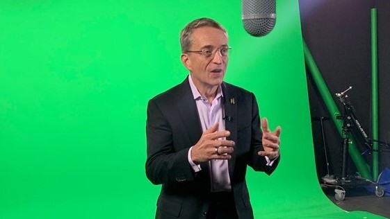
"The continued proliferation of technology is driving sustained, long-term demand for semiconductors, creating a $1 trillion market opportunity by 2030," said Pat Gelsinger, Intel chief executive officer. "With that opportunity in mind, today we outlined our strategy and roadmap for accelerating to 10%-12% year-over-year revenue growth by 2026 by doubling down on innovation, driving even deeper collaboration with our customers and partners, and leveraging our core strengths to successfully grow traditional markets and disrupt new ones. Our goals are ambitious, but I'm confident we have the right strategy and right team to achieve them and to deliver long-term value for our shareholders."


"The continued proliferation of technology is driving sustained, long-term demand for semiconductors, creating a $1 trillion market opportunity by 2030," said Pat Gelsinger, Intel chief executive officer. "With that opportunity in mind, today we outlined our strategy and roadmap for accelerating to 10%-12% year-over-year revenue growth by 2026 by doubling down on innovation, driving even deeper collaboration with our customers and partners, and leveraging our core strengths to successfully grow traditional markets and disrupt new ones. Our goals are ambitious, but I'm confident we have the right strategy and right team to achieve them and to deliver long-term value for our shareholders."