News Posts matching #SRAM

Return to Keyword Browsing

TSMC Boosts 2 nm Yields by 6%, Passing Savings to Customers

Being the leading-edge semiconductor manufacturing company, TSMC actively works on increasing the efficiency of its upcoming nodes, even when they are finalized and ready for high-volume manufacturing. According to a TSMC employee identified as Dr. Kim on X, recent test runs of the 2 nm N2 nodes show a 6% improvement in production yields compared to baseline expectations. This advancement could translate into substantial cost savings for the company's customers when mass production begins in late 2025. However, specific details about whether the gains were achieved in SRAM or logic test chips remain undisclosed. The timing is particularly noteworthy as TSMC prepares to launch its shuttle test wafer services for 2 nm technology in January. The N2 process represents a giant leap for TSMC, marking its first gate-all-around (GAA) nanosheet transistors implementation, the first step to derive from the classical FinFET design.

According to TSMC's projections, chips manufactured using the N2 process will consume 25-30% less power while maintaining the same transistor count and frequency as its N3E node. Additionally, the technology is expected to deliver 10-15% performance improvements and achieve a 15% increase in transistor density. A key innovation in the N2 process is the enhanced design of its GAA nanosheet transistors, which offers improved electrostatic control and reduced gate leakage compared to 3 nm FinFET transistors, given that the gate can be controlled from all sides. This advancement enables smaller high-density transistors to maintain reliable performance through better threshold voltage tuning capabilities. With approximately seven to eight months until full-scale volume production begins, the company has a substantial window to optimize the manufacturing process further and potentially achieve additional yield improvements, although that is less likely.
AMD Ryzen 7 9800X3D Overclocked to 5.46 GHz, Beating Ryzen 7 7800X3D by 27%

We are days away from the official November 7 launch of AMD's Ryzen 7 9800X3D CPU with 3D V-Cache, and we are already seeing some estimates of the speedup compared to the last-generation Ryzen 7 7800X3D CPU. According to a Geekbench submission discovered by Everest (Olrak29_) on X, the upcoming AMD Ryzen 7 9800X3D has been spotted running at a clock speed of 5.46 GHz. This is a 260 MHz increase from the official boost frequency of 5.2 GHz, which indicates overclocking has been applied. If readers recall, the last generations of X3D processors had overclocking disabled, and this time, things are looking different thanks to the compute die being placed on top of SRAM. AMD attributes this to CCD being closer to the heat spreader instead of memory and allowing it to spread heat more effectively, ensuring a stable overclock.

Regarding performance, the Ryzen 7 9800X3D outperforms its predecessor, the Ryzen 7 7800X3D, by an impressive 27.4% in the single-core Geekbench v6 test and 26.8% in the multicore test. The last generation CPU scored 2,726 points in single-core and 15,157 points in multicore tests, while the new Zen 5 design has managed to produce 3,473 points in single-core and 19,216 in multicore tests. These results are approximately 27% improvement over the Zen 4, suggesting that the Zen 5 architecture benefits greatly from better SRAM bandwidth and capacity. While these results only come from synthetic benchmarks, they give us a picture of what to expect from this CPU. We have to wait for more real-world test cases to fully conclude the improvement factor.

Intel Launches Gaudi 3 AI Accelerator: 70% Faster Training, 50% Faster Inference Compared to NVIDIA H100, Promises Better Efficiency Too

During the Vision 2024 event, Intel announced its latest Gaudi 3 AI accelerator, promising significant improvements over its predecessor. Intel claims the Gaudi 3 offers up to 70% improvement in training performance, 50% better inference, and 40% better efficiency than Nvidia's H100 processors. The new AI accelerator is presented as a PCIe Gen 5 dual-slot add-in card with a 600 W TDP or an OAM module with 900 W. The PCIe card has the same peak 1,835 TeraFLOPS of FP8 performance as the OAM module despite a 300 W lower TDP. The PCIe version works as a group of four per system, while the OAM HL-325L modules can be run in an eight-accelerator configuration per server. This likely will result in a lower sustained performance, given the lower TDP, but it confirms that the same silicon is used, just finetuned with a lower frequency. Built on TSMC's N5 5 nm node, the AI accelerator features 64 Tensor Cores, delivering double the FP8 and quadruple FP16 performance over the previous generation Gaudi 2.

The Gaudi 3 AI chip comes with 128 GB of HBM2E with 3.7 TB/s of bandwidth and 24 200 Gbps Ethernet NICs, with dual 400 Gbps NICs used for scale-out. All of that is laid out on 10 tiles that make up the Gaudi 3 accelerator, which you can see pictured below. There is 96 MB of SRAM split between two compute tiles, which acts as a low-level cache that bridges data communication between Tensor Cores and HBM memory. Intel also announced support for the new performance-boosting standardized MXFP4 data format and is developing an AI NIC ASIC for Ultra Ethernet Consortium-compliant networking. The Gaudi 3 supports clusters of up to 8192 cards, coming from 1024 nodes comprised of systems with eight accelerators. It is on track for volume production in Q3, offering a cost-effective alternative to NVIDIA accelerators with the additional promise of a more open ecosystem. More information and a deeper dive can be found in the Gaudi 3 Whitepaper.

Groq LPU AI Inference Chip is Rivaling Major Players like NVIDIA, AMD, and Intel

AI workloads are split into two different categories: training and inference. While training requires large computing and memory capacity, access speeds are not a significant contributor; inference is another story. With inference, the AI model must run extremely fast to serve the end-user with as many tokens (words) as possible, hence giving the user answers to their prompts faster. An AI chip startup, Groq, which was in stealth mode for a long time, has been making major moves in providing ultra-fast inference speeds using its Language Processing Unit (LPU) designed for large language models (LLMs) like GPT, Llama, and Mistral LLMs. The Groq LPU is a single-core unit based on the Tensor-Streaming Processor (TSP) architecture which achieves 750 TOPS at INT8 and 188 TeraFLOPS at FP16, with 320x320 fused dot product matrix multiplication, in addition to 5,120 Vector ALUs.

Having massive concurrency with 80 TB/s of bandwidth, the Groq LPU has 230 MB capacity of local SRAM. All of this is working together to provide Groq with a fantastic performance, making waves over the past few days on the internet. Serving the Mixtral 8x7B model at 480 tokens per second, the Groq LPU is providing one of the leading inference numbers in the industry. In models like Llama 2 70B with 4096 token context length, Groq can serve 300 tokens/s, while in smaller Llama 2 7B with 2048 tokens of context, Groq LPU can output 750 tokens/s. According to the LLMPerf Leaderboard, the Groq LPU is beating the GPU-based cloud providers at inferencing LLMs Llama in configurations of anywhere from 7 to 70 billion parameters. In token throughput (output) and time to first token (latency), Groq is leading the pack, achieving the highest throughput and second lowest latency.

AMD 3D V-Cache RAM Disk Delivers Over 182 GB/s and 175 GB/s Read and Write Speeds

AMD's 3D V-Cache technology utilizes blocks of SRAM stacked on top of the CPU logic die, where CPU cores reside, and allows the processor to access massive pools of cache for applications. However, using this extra level 3 (L3) cache as a RAM disk appears possible, where the L3 SRAM behaves similarly to a storage drive. A big disclaimer here is that this is only possible by exposing the L3 to the CrystalDiskMark benchmark, and no real-world applications can do it in a way that CrystalDiskMark. According to X/Twitter user Nemez (@GPUsAreMagic), the steps to replicate this procedure are: Obtaining an AMD Ryzen CPU with 3D V-Cache, installing OSFMount and creating a FAT32 formatted RAM disk, and running CrystalDiskMark, with values set to values to SEQ 256 KB, Queue Depth 1, Threads 16, and data fill to 0s instead of random.

The results of this experiment? Well, they appear to be rather stunning as the nature of L3 SRAM is that the memory is tiny but very fast and accessible to the CPU, so it can help load data locally before going to the system RAM. With AMD Ryzen 7 5800X3D, the speeds of this RAM disk are over 182 GB/s for reading and over 175 GB/s for writing. In another test, shared by Albert Thomas (@ultrawide219), we managed to see RAM disk based on AMD Ryzen 7800X3D V-Cache, which scores a little less with over 178 GB/s read and over 163 GB/s write speeds. Again, CrystalDiskMark only performed these tests on small allocations varying between 16 MiB and 32 MiB, so no real-world workloads are yet able to utilize this.

Zero ASIC Democratizing Chip Making

Zero ASIC, a semiconductor startup, came out of stealth today to announce early access to its one-of-a-kind ChipMaker platform, demonstrating a number of world firsts:
  • 3D chiplet composability enabling billions of new silicon products
  • Fully automated no-code chiplet-based chip design
  • Zero install interactive RTL-based chip emulation
  • Roadmap to 100X reduction in chip development costs
"Custom Application Specific Integrated Circuits (ASICs) offer 10-100X cost and energy advantage over commercial off the shelf (COTS) devices, but the enormous development cost makes ASICs non-viable for most applications," said Andreas Olofsson, CEO and founder of Zero ASIC. "To build the next wave of world changing silicon devices, we need to reduce the barrier to ASICs by orders of magnitude. Our mission at Zero ASIC is to make ordering an ASIC as easy as ordering catalog parts from an electronics distributor."

Fujitsu Details Monaka: 150-core Armv9 CPU for AI and Data Center

Ever since the creation of A64FX for the Fugaku supercomputer, Fujitsu has been plotting the development of next-generation CPU design for accelerating AI and general-purpose HPC workloads in the data center. Codenamed Monaka, the CPU is the latest creation for TSMC's 2 nm semiconductor manufacturing node. Based on Armv9-A ISA, the CPU will feature up to 150 cores with Scalable Vector Extensions 2 (SVE2), so it can process a wide variety of vector data sets in parallel. Using a 3D chiplet design, the 150 cores will be split into different dies and placed alongside SRAM and I/O controller. The current width of the SVE2 implementation is unknown.

The CPU is designed to support DDR5 memory and PCIe 6.0 connection for attaching storage and other accelerators. To bring cache coherency among application-specific accelerators, CXL 3.0 is present as well. Interestingly, Monaka is planned to arrive in FY2027, which starts in 2026 on January 1st. The CPU will supposedly use air cooling, meaning the design aims for power efficiency. Additionally, it is essential to note that Monaka is not a processor that will power the post-Fugaku supercomputer. The post-Fugaku supercomputer will use post-Monaka design, likely iterating on the design principles that Monaka uses and refining them for the launch of the post-Fugaku supercomputer scheduled for 2030. Below are the slides from Fujitsu's presentation, in Japenese, which highlight the design goals of the CPU.

TSMC Announces Breakthrough Set to Redefine the Future of 3D IC

TSMC today announced the new 3Dblox 2.0 open standard and major achievements of its Open Innovation Platform (OIP) 3DFabric Alliance at the TSMC 2023 OIP Ecosystem Forum. The 3Dblox 2.0 features early 3D IC design capability that aims to significantly boost design efficiency, while the 3DFabric Alliance continues to drive memory, substrate, testing, manufacturing, and packaging integration. TSMC continues to push the envelope of 3D IC innovation, making its comprehensive 3D silicon stacking and advanced packaging technologies more accessible to every customer.

"As the industry shifted toward embracing 3D IC and system-level innovation, the need for industry-wide collaboration has become even more essential than it was when we launched OIP 15 years ago," said Dr. L.C. Lu, TSMC fellow and vice president of Design and Technology Platform. "As our sustained collaboration with OIP ecosystem partners continues to flourish, we're enabling customers to harness TSMC's leading process and 3DFabric technologies to reach an entirely new level of performance and power efficiency for the next-generation artificial intelligence (AI), high-performance computing (HPC), and mobile applications."

TSMC N3 Nodes Show SRAM Scaling is Hitting the Wall

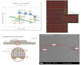
When TSMC introduced its N3 lineup of nodes, the company only talked about the logic scaling of the two new semiconductor manufacturing steps. However, it turns out that there was a reason for it, as WikiChip confirms that the SRAM bit cells of N3 nodes are almost identical to the SRAM bit cells of N5 nodes. At TSMC 2023 Technology Symposium, TSMC presented additional details about its N3 node lineup, including logic and SRAM density. For starters, the N3 node is TSMC's "3 nm" node family that has two products: a Base N3 node (N3B) and an Enhanced N3 node (N3E). The base N3B uses a new (for TSMC) self-aligned contact (SAC) scheme that Intel introduced back in 2011 with a 22 nm node, which improves the node's yield.

Regardless of N3's logic density improvements compared to the "last-generation" N5, the SRAM density is almost identical. Initially, TSMC claimed N3B SRAM density was 1.2x over the N5 process. However, recent information shows that the actual SRAM density is merely a 5% difference. With SRAM taking a large portion of the transistor and area budget of a processor, N3B's soaring manufacturing costs are harder to justify when there is almost no area improvement. For some time, SRAM scaling wasn't following logic scaling; however, the two have now completely decoupled.

Samsung to Detail SF4X Process for High-Performance Chips

Samsung has invested heavily in semiconductor manufacturing technology to provide clients with a viable alternative to TSMC and its portfolio of nodes spanning anything from mobile to high-performance computing (HPC) applications. Today, we have information that Samsung will present its SF4X node to the public in this year's VLSI Symposium. Previously known as a 4HPC node, it is designed as a 4 nm-class node with a specialized use case for HPC processors, in contrast to the standard SF4 (4LPP) node that uses 4 nm transistors designed for low-power standards applicable to mobile/laptop space. According to the VLSI Symposium schedule, Samsung is set to present more info about the paper titled "Highly Reliable/Manufacturable 4nm FinFET Platform Technology (SF4X) for HPC Application with Dual-CPP/HP-HD Standard Cells."

As the brief introduction notes, "In this paper, the most upgraded 4nm (SF4X) ensuring HPC application was successfully demonstrated. Key features are (1) Significant performance +10% boosting with Power -23% reduction via advanced SD stress engineering, Transistor level DTCO (T-DTCO) and [middle-of-line] MOL scheme, (2) New HPC options: Ultra-Low-Vt device (ULVT), high speed SRAM and high Vdd operation guarantee with a newly developed MOL scheme. SF4X enhancement has been proved by a product to bring CPU Vmin reduction -60mV / IDDQ -10% variation reduction together with improved SRAM process margin. Moreover, to secure high Vdd operation, Contact-Gate breakdown voltage is improved by >1V without Performance degradation. This SF4X technology provides a tremendous performance benefits for various applications in a wide operation range." While we have no information on the reference for these claims, we suspect it is likely the regular SF4 node. More performance figures and an in-depth look will be available on Thursday, June 15, at Technology Session 16 at the symposium.

Habana Labs Launches Second-generation AI Deep Learning Processors

Today at the Intel Vision conference, Habana Labs, an Intel company, announced its second-generation deep learning processors, the Habana Gaudi 2 Training and Habana Greco Inference processors. The processors are purpose-built for AI deep learning applications, implemented in 7nm technology and build upon Habana's high-efficiency architecture to provide customers with higher-performance model training and inferencing for computer vision and natural language applications in the data center. At Intel Vision, Habana Labs revealed Gaudi2's training throughput performance for the ResNet-50 computer vision model and the BERT natural language processing model delivers twice the training throughput over the Nvidia A100-80GB GPU.

"The launch of Habana's new deep learning processors is a prime example of Intel executing on its AI strategy to give customers a wide array of solution choices - from cloud to edge - addressing the growing number and complex nature of AI workloads. Gaudi2 can help Intel customers train increasingly large and complex deep learning workloads with speed and efficiency, and we're anticipating the inference efficiencies that Greco will bring."—Sandra Rivera, Intel executive vice president and general manager of the Datacenter and AI Group

ATP Announces High-Endurance 3D TLC-based eMMC Devices

ATP Electronics, the global leader in specialized storage and memory solutions, has introduced its latest line of e.MMC devices built on 3D triple level cell (TLC) NAND. Using a new die package, the E750Pi/Pc and E650Si/Sc Series offer long-life performance, optimized power consumption and customizable configuration options. ATP's new E750Pi/Pc Series e.MMC offerings are built with 3D TLC NAND flash but are configured as pseudo SLC (pSLC) to offer endurance on par with SLC NAND, while E650Si/Sc Series in native TLC has near-MLC endurance.

The E750Pi and E650Si Series are industrial temperature-operable (-40°C to 85°C), making them ideal for deployment in scenarios with extreme thermal challenges and harsh environments, while E750Pc and E650Sc support -25°C to 85°C operating temperatures for applications with non-critical thermal requirements.

Intel Details Ponte Vecchio Accelerator: 63 Tiles, 600 Watt TDP, and Lots of Bandwidth

During the International Solid-State Circuits Conference (ISSCC) 2022, Intel gave us a more significant look at its upcoming Ponte Vecchio HPC accelerator and how it operates. So far, Intel convinced us that the company created Ponte Vecchio out of 47 tiles glued together in one package. However, the ISSCC presentation shows that the accelerator is structured rather interestingly. There are 63 tiles in total, where 16 are reserved for compute, eight are used for RAMBO cache, two are Foveros base tiles, two represent Xe-Link tiles, eight are HBM2E tiles, and EMIB connection takes up 11 tiles. This totals for about 47 tiles. However, an additional 16 thermal tiles used in Ponte Vecchio regulate the massive TDP output of this accelerator.

What is interesting is that Intel gave away details of the RAMBO cache. This novel SRAM technology uses four banks of 3.75 MB groups total of 15 MB per tile. They are connected to the fabric at 1.3 TB/s connection per chip. In contrast, compute tiles are connected at 2.6 TB/s speeds to the chip fabric. With eight RAMBO cache tiles, we get an additional 120 MB SRAM present. The base tile is a 646 mm² die manufactured in Intel 7 semiconductor process and contains 17 layers. It includes a memory controller, the Fully Integrated Voltage Regulators (FIVR), power management, 16-lane PCIe 5.0 connection, and CXL interface. The entire area of Ponte Vecchio is rather impressive, as 47 active tiles take up 2,330 mm², whereas when we include thermal dies, the total area jumps to 3,100 mm². And, of course, the entire package is much larger at 4,844 mm², connected to the system with 4,468 pins.

AMD Readying 16-core "Zen 4" CCDs Exclusively for the Client Segment with an Answer to Intel E-cores?

AMD already declared the CPU core counts of its EPYC "Genoa" and "Bergamo" processors to top out at 96 and 128, respectively, a core-count believed to have been facilitated by the larger fiberglass substrate of the next-gen SP5 CPU socket, letting AMD add more 8-core "Zen 4" chiplets, dubbed CPU complex dies (CCDs). Until now, AMD has used the chiplet as a common component between its EPYC enterprise and Ryzen desktop processors, to differentiate CPU core counts.

A fascinating theory that hit the rumor-mill, indicates that the company might leverage 5 nm (TSMC N5) carve out larger CCDs with up to 16 "Zen 4" CPU cores. Half of these cores are capped at a much lower power budget, essentially making them efficient-cores. This is a concept AMD appears to be carrying over from its 15-Watt class mobile processors, which see the CPU cores operate under an aggressive power-management. These cores still turn out a reasonable amount of performance, and are functionally identical to the ones on 105 W desktop processors with a relaxed power budget.

AMD "Zen 3" 3D Vertical Cache Detailed Some More

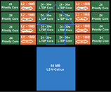
Senior Technology Fellow Yuzo Fukuzaki shed light on the elusive new CPU technology AMD unveiled at its Computex 2021 keynote, 3D Vertical Cache (3DV Cache). The company had then detailed it as an additional 64 MB last-level cache stacked on top of a CCD (CPU core complex die), which significantly improves performance, including a claimed 15% average gain in gaming performance, which accounts for a generational performance gain over "Zen 3." The prototype AMD unveiled in its keynote was based on a Socket AM4 processor with "Zen 3" CCDs that have the 3DV Cache components in place. With two such CCDs, a 16-core processor would end up with 192 MB of L3 cache.

Yuzo Fukuzaki's theory sheds light on the most plausible position of 3DV Cache in the processor's cache hierarchy. Apparently, it expands the CCD's L3 cache, and doesn't serve as an "L4" victim cache to the L3. This way, the cache setup remains transparent to the OS, which sees it as a contiguous 96 MB block of L3 cache (per CCD). The 3DV Cache die is an SRAM chip fabricated on the same 7 nm process as the "Zen 3" CCD. It measures 6 mm x 6 mm (36 mm²), and is located above the region of the CCD that typically has the 32 MB L3 SRAM. Fukuzaki estimates that roughly 23,000 TSVs (through-silicon vias), each about 17 µm in size, connect the 3DV Cache die to the main CCD.

Samsung Demonstrates 256 Gb 3 nm MBCFET Chip at ISSCC 2021

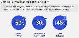
During the IEEE International Solid-State Circuits Conference (ISSCC), Samsung Foundry has presented a new step towards smaller and more efficient nodes. The new chip that was presented is a 256 Gb memory chip, based on SRAM technology. However, all of that doesn't sound interesting, until we mention the technology that is behind it. Samsung has for the first time manufactured a chip using the company's gate-all-around field-effect transistor (GAAFET) technology on the 3 nm semiconductor node. Formally, there are two types of GAAFET technology: the regular GAAFET that uses nanowires as fins of the transistor, and MBCFET (multi-bridge channel FET) that uses thicker fins that come in a form of a nanosheet.

Samsung has demonstrated the first SRAM chip that uses MBCFET technology today. The chip in question is a 256 Gb chip with an area of 56 mm². The achievement Samsung is proud of is that the chip uses 230 mV less power for writes, compared to the standard approach, as the MBCFET transistors allow the company to have many different power-saving techniques. The new 3 nm MBCFET process is expected to get into high-volume production sometime in 2022, however, we are yet to see demos of logic chips besides SRAM like we see today. Nonetheless, even the demonstration of SRAM is big progress, and we are eager to see what the company manages to build with the new technology.

TSMC Announces the N12e Enhanced 12nm FF Node for 5G and IoT Edge Devices

TSMC on Monday announced the N12e silicon fabrication node. An enhancement of its 12 nm FinFET node, N12e is designed for value 5G application processors, MODEMs, and IoT edge devices, such as true-wireless earbuds, smartwatch processors, wearables, VR HMDs, entry-level and mainstream SoCs, etc. The node has been derived from the company's 12FFC+_ULL node, and fits into the 12-16 nm class of nodes. It's intended to succeed the company's 22ULL node (in terms of pricing), offering a 76% increase in logic density, 49% increase in clock speed at a given power, 55% improvement in power draw at a given speed, 50% reduction in SRAM leakage current, and low Vdd, with support for logic voltages as low as 0.4 V. That last bit in particular should make the node suitable for tiny, battery-powered devices such as wearables.

Samsung Announces Availability of its Silicon-Proven 3D IC Technology

Samsung Electronics Co., Ltd., a world leader in advanced semiconductor technology, today announced the immediate availability of its silicon-proven 3D IC packaging technology, eXtended-Cube (X-Cube), for today's most advanced process nodes. Leveraging Samsung's through-silicon via (TSV) technology, X-Cube enables significant leaps in speed and power efficiency to help address the rigorous performance demands of next-generation applications including 5G, artificial intelligence, high-performance computing, as well as mobile and wearable.

"Samsung's new 3D integration technology ensures reliable TSV interconnections even at the cutting-edge EUV process nodes," said Moonsoo Kang, senior vice president of Foundry Market Strategy at Samsung Electronics. "We are committed to bringing more 3D IC innovation that can push the boundaries of semiconductors."

Everspin Technologies and GLOBALFOUNDRIES Extend MRAM Joint Development Agreement to 12nm

Everspin Technologies, Inc., the world's leading developer and manufacturer of Magnetoresistive RAM (MRAM), today announced an amendment of its Spin-transfer Torque (STT-MRAM) joint development agreement (JDA) with GLOBALFOUNDRIES (GF ), the world's leading specialty foundry. Everspin and GF have been partners on 40 nm, 28 nm, and 22 nm STT-MRAM development and manufacturing processes and have now updated their agreement to set the terms for a future project on an advanced 12 nm FinFET MRAM solution. Everspin is in production of discrete STT-MRAM solutions on 40 and 28 nm, including its award winning 1 Gb DDR4 device. GF recently announced it has achieved initial production of embedded MRAM (eMRAM) on its 22FDX platform.

GLOBALFOUNDRIES Introduces 12LP+ FinFET Solution for Cloud and Edge AI Applications

GLOBALFOUNDRIES (GF), the world's leading specialty foundry, announced today at its Global Technology Conference the availability of 12LP+, an innovative new solution for AI training and inference applications. 12LP+ offers chip designers a best-in-class combination of performance, power and area, along with a set of key new features, a mature design and production ecosystem, cost-efficient development and fast time-to-market for high-growth cloud and edge AI applications.

Derived from GF's existing 12nm Leading Performance (12LP) platform, GF's new 12LP+ provides either a 20% increase in performance or a 40% reduction in power requirements over the base 12LP platform, plus a 15% improvement in logic area scaling. A key feature is a high-speed, low-power 0.5 V SRAM bit cell that supports the fast, power-efficient shuttling of data between processors and memory, an important requirement for AI applications in the computing and wired infrastructure markets.

AMD Details ZEN Microarchitecture IPC Gains

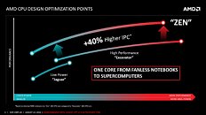
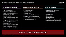
AMD Tuesday hosted a ZEN microarchitecture deep-dive presentation in the backdrop of Hot Chips, outlining its road to a massive 40 percent gain in IPC (translated roughly as per-core performance gains), over the current "Excavator" microarchitecture. The company credits the gains to three major changes with ZEN: better core engine, better cache system, and lower power. With ZEN, AMD pulled back from its "Bulldozer" approach to cores, in which two cores share certain number-crunching components to form "modules," and back to a self-sufficient core design.

Beyond cores, the next-level subunit of the ZEN architecture is the CPU-Complex (CCX), in which four cores share an 8 MB L3 cache. This isn't different from current Intel architectures, the cores share nothing beyond L3 cache, making them truly independent. What makes ZEN a better core, besides its independence from other cores, and additional integer pipelines; subtle upscaling in key ancillaries such as micro-Op dispatch, instruction schedulers; retire, load, and store queues; and a larger quad-issue FPU.

Xbox One Chip Slower Than PlayStation 4

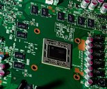
After bagging chip supply deals for all three new-generation consoles -- Xbox One, PlayStation 4, and Wii U, things are looking up for AMD. While Wii U uses older-generation hardware technologies, Xbox One and PlayStation 4 use the very latest AMD has to offer -- "Jaguar" 64-bit x86 CPU micro-architecture, and Graphics CoreNext GPU architecture. Chips that run the two consoles have a lot in common, but also a few less-than-subtle differences.

PlayStation 4 chip, which came to light this February, is truly an engineer's fantasy. It combines eight "Jaguar" 64-bit x86 cores clocked at 1.60 GHz, with a fairly well spec'd Radeon GPU, which features 1,156 stream processors, 32 ROPs; and a 256-bit wide unified GDDR5 memory interface, clocked at 5.50 GHz. At these speeds, the system gets a memory bandwidth of 176 GB/s. Memory isn't handled like UMA (unified memory architecture), there's no partition between system- and graphics-memory. The two are treated as items on the same 8 GB of memory, and either can use up a majority of it.

Fujitsu and SuVolta Demo ULV Operation of SRAM Down to ~0.4V

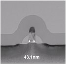
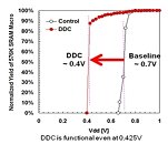
Fujitsu Semiconductor Limited and SuVolta, Inc. today announced that they have successfully demonstrated ultra-low-voltage operation of SRAM (static random access memory) blocks down to 0.425V by integrating SuVolta's PowerShrink low-power CMOS platform into Fujitsu Semiconductor's low-power process technology. By reducing power consumption, these technologies will make possible the ultimate in "ecological" products in the near future. Technology details and results will be presented at the 2011 International Electron Devices Meeting (IEDM) being held in Washington DC, starting December 5th.

Controlling power consumption is the primary limiter of adding features to product types ranging from mobile electronics to tethered servers and networking equipment. The biggest contributor to power consumption is supply voltage. Previously, the power supply voltage of CMOS steadily reduced to approximately 1.0V at the 130nm technology node, but it has not reduced much further as technology has scaled to the 28nm node. To reduce the power supply voltage, one of the biggest obstacles is the minimum operating voltage of embedded SRAM blocks.

Toshiba Launches Highest Density Embedded NAND Flash Memory Devices

Toshiba Corp. (Toshiba) and Toshiba America Electronic Components, Inc. (TAEC), its subsidiary in the Americas, today announced the launch of a 64 gigabyte (GB) embedded NAND flash memory module, the highest capacity yet achieved in the industry. The chip is the flagship device in a line-up of six new embedded NAND flash memory modules that offer full compliance with the latest e-MMC standard, and that are designed for application in a wide range of digital consumer products, including Smartphones, mobile phones, netbooks and digital video cameras. Samples of the 64GB module are available from today, and mass production will start in the first quarter of 2010.

The new 64GB embedded device combines sixteen pieces of 32Gbit (equal to 4GB) NAND chips fabricated with Toshiba's cutting-edge 32nm process technology, and also integrates a dedicated controller. Toshiba is the first company to succeed in combining 16 pieces of 32Gbit NAND chips, and applied advanced chip thinning and layering technologies to realize individual chips that are only 30 micrometers thick. Full compliance with the JEDEC/MMCA Version 4.4(V4.4) standard for embedded MultiMediaCards supports standard interfacing and simplifies embedding in products, reducing development burdens on product manufacturers. Toshiba offers a comprehensive line-up of single-package embedded NAND Flash memories in densities ranging from 2GB to 64GB. All integrate a controller to manage basic control functions for NAND applications, and are compatible with the latest e-MMC standard and its new features, including defining multiple storage areas and enhanced security features.

GLOBALFOUNDRIES To Highlight 32nm/28nm Technology Leadership at GSA Expo

As the semiconductor industry begins its transition to the next technology node, GLOBALFOUNDRIES is on track to take its position as the foundry technology leader. On October 1 at the Global Semiconductor Alliance Emerging Opportunities Expo & Conference in Santa Clara, Calif., GLOBALFOUNDRIES (Booth 321) will provide the latest details on its technology roadmap for the 32nm/28nm generations and its innovative "Gate First" approach to building transistors based on High-K Metal Gate (HKMG) technology.

"With each new technology generation, semiconductor foundries are increasingly challenged with the economics to sustain R&D and the know-how to bring these technologies to market in high-volume," said Len Jelinek, director and chief analyst, iSuppli. "With a heritage of rapidly ramping leading-edge technologies to high volumes at mature yields, combined with aggressive investments in capacity and technology, GLOBALFOUNDRIES is uniquely-positioned to challenge for next-generation foundry leadership."
Return to Keyword Browsing
Jan 21st, 2025 04:51 EST change timezone

New Forum Posts

Popular Reviews

Controversial News Posts