Friday, August 6th 2021

AMD "Zen 3" 3D Vertical Cache Detailed Some More
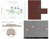
Senior Technology Fellow Yuzo Fukuzaki shed light on the elusive new CPU technology AMD unveiled at its Computex 2021 keynote, 3D Vertical Cache (3DV Cache). The company had then detailed it as an additional 64 MB last-level cache stacked on top of a CCD (CPU core complex die), which significantly improves performance, including a claimed 15% average gain in gaming performance, which accounts for a generational performance gain over "Zen 3." The prototype AMD unveiled in its keynote was based on a Socket AM4 processor with "Zen 3" CCDs that have the 3DV Cache components in place. With two such CCDs, a 16-core processor would end up with 192 MB of L3 cache.
Yuzo Fukuzaki's theory sheds light on the most plausible position of 3DV Cache in the processor's cache hierarchy. Apparently, it expands the CCD's L3 cache, and doesn't serve as an "L4" victim cache to the L3. This way, the cache setup remains transparent to the OS, which sees it as a contiguous 96 MB block of L3 cache (per CCD). The 3DV Cache die is an SRAM chip fabricated on the same 7 nm process as the "Zen 3" CCD. It measures 6 mm x 6 mm (36 mm²), and is located above the region of the CCD that typically has the 32 MB L3 SRAM. Fukuzaki estimates that roughly 23,000 TSVs (through-silicon vias), each about 17 µm in size, connect the 3DV Cache die to the main CCD.
Sources:
Yuzo Fukuzaki (Linkedin), Retired Engineer (Twitter)
Yuzo Fukuzaki's theory sheds light on the most plausible position of 3DV Cache in the processor's cache hierarchy. Apparently, it expands the CCD's L3 cache, and doesn't serve as an "L4" victim cache to the L3. This way, the cache setup remains transparent to the OS, which sees it as a contiguous 96 MB block of L3 cache (per CCD). The 3DV Cache die is an SRAM chip fabricated on the same 7 nm process as the "Zen 3" CCD. It measures 6 mm x 6 mm (36 mm²), and is located above the region of the CCD that typically has the 32 MB L3 SRAM. Fukuzaki estimates that roughly 23,000 TSVs (through-silicon vias), each about 17 µm in size, connect the 3DV Cache die to the main CCD.

46 Comments on AMD "Zen 3" 3D Vertical Cache Detailed Some More
On the other hand, next gen APUs, with Zen 4 cores, RDNA1/2 iGPUs, infinity cache and 3D cache, could make today's APUs look like old and very slow trash. Like comparing an AM4 APU with an FM2+ APU.
I'm much more concerned about cost and availability, the latter of which has been a huge limitation for AMD lately.
With that said, I think that pricing is going to be really bad for those Zen3D parts and only for 5900X and 5950X, any lower and it kinda stops making sense.
One random thought that I had was what if AMD plan is to remove L3 cache altogether from the CCD and only have it from the cache die. That could be good for yields as reduces the CCD die considerably(a cache die would also likely be defect resistant since SRAM is easily redundant and thus possibly cheap), though It depends on how costly the 3D packaging is and others factors that I am probably unaware of that could make this unviable. For temperatures, maybe use some of those new 3D packaging tech that allows you to put logic on top. Could also use this as a bridge between CCDs like in the RDNA3 rumours?
That's just a random thought of mine though and probably completely wrong, so just ignore it.
Did you expect a skyscraper?
I mean at 7nm it probably scales like a skyscraper.
Cache is the new performance booster, Infonity cache, 3DV cache, the M1.
What are you worried about?
3D chip is not there yet and not around the corner (if it ever come). Right now it's each die are in 2D. they can stack those and have TSV, but it remain that each layer is 2D. 3D will allow very complex transistor layout. It would help with propagation as you would be able to make denser logic with less space. But I am still not even sure we can make those in labs...
Anyway, that do not mean that this 3D cache isn't impressive. It's actually very impressive and only the beginning of die stacking. The next decade will be very interesting, trust me on that. This is only the beginning.
L3 is a spillover cache for L2. Boosting L3 cache will help reduce cache misses, but probably mostly cache lines with instructions, as discarded data cache lines are less likely to be reused quickly, which means the gains will be very workload dependent. But regardless this is a very expensive way to add a little performance. This makes me wonder if this will be reserved for a small selection of premium models.
Cooling is not an issue.
Source: AMD NDA docs.
But Amd said that: