News Posts matching #Raven Ridge

Return to Keyword Browsing

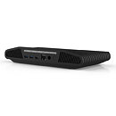
Atari VCS Console Finally Set To Release in Fall 2020 for $389.99 USD

The Atari VCS was first announced over two years ago in 2018 but has since suffered numerous delays. It looks like there may be light at the end of the tunnel for the Atari VCS 800 with the console now available for pre-order from Atari, GameStop, or Walmart. The console is only available as part of a bundle including the console itself, Wireless Classic Joystick, a Modern Controller, and free copy of Atari Vault of 100 classic arcade and console games. The bundle is priced at 389.99 USD and is expected to ship by the 2020 holiday season.

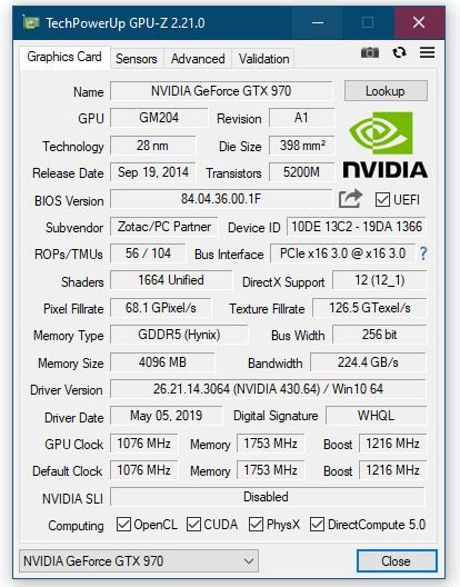
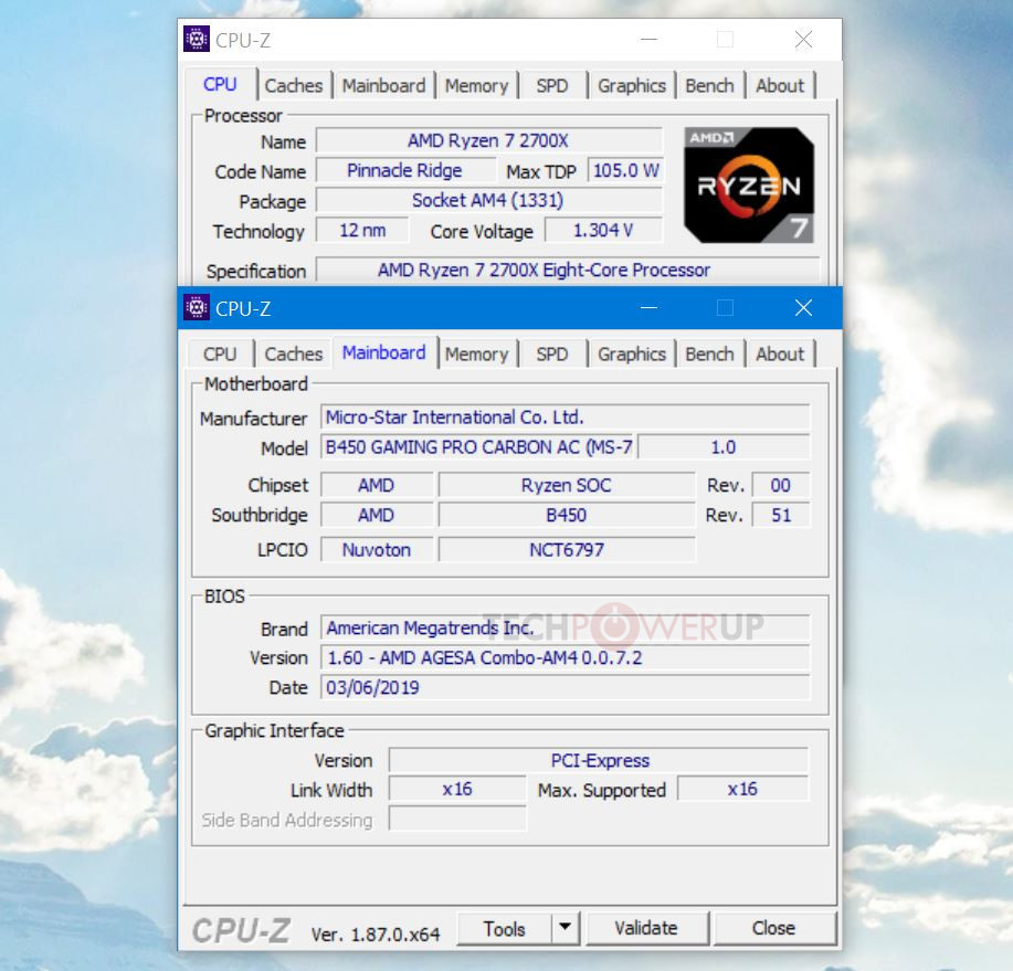
The console features a custom AMD Raven Ridge APU with Vega 3 graphics, paired with 8 GB DDR4 ram, and 32 GB eMMC internal flash storage. The device runs a custom Linux OS but also supports Linux, Windows, Steam OS, or Chrome OS if booting from an external drive. Connectivity consists of 802.11 b/g/n Wi-Fi, and Bluetooth 4.0 while I/O includes a single HDMI 2.0 port, gigabit Ethernet port, and quad USB 3.1 connectors. A lower-powered Atari VCS 400 system is also planned with half the ram at 4 GB and is expected to sell for 249.99 USD.

AMD "Renoir" Die Annotation Raises Hopes of Desktop Chips Featuring x16 PEG

VLSI engineer Fritzchens Fritz, famous for high-detail EM photography of silicon dies and annotations of them, recently published his work on AMD's 7 nm "Renoir" APU silicon. His die-shots were annotated by Nemez aka GPUsAreMagic. The floor-plan of the silicon shows that the CPU component finally dwarfs the iGPU component, thanks to double the CPU cores over the previous-gen "Picasso" silicon, spread over two CCXs (compute complexes). The CCX on "Renoir" is visibly smaller than the one on the "Zen 2" CCDs found in "Matisse" and "Rome" MCMs, as the L3 cache is smaller, at 4 MB compared to 16 MB. Being MCMs with disintegrated memory controllers, it makes more sense for CCDs to have more last-level cache per CCX.

We also see that the iGPU features no more than 8 "Vega" NGCUs, so there's no scope for "Renoir" based desktop APUs to feature >512 stream processors. AMD attempted to compensate for the NGCU deficit by dialing up engine clocks of the iGPU by over 40% compared to those on "Picasso." What caught our eye in the annotation is the PCI-Express physical layer. Apparently the die indeed has 20 PCI-Express lanes besides an additional 4 lanes that can be configured as two SATA 6 Gbps ports thanks to SerDes flexibility.

AMD Releases Athlon 3000G Low-cost Desktop Processor

AMD today released its Athlon 3000G low-cost desktop processor to cap off its entry-level. Based on the 14 nm "Raven Ridge" silicon, the chip combines a 2-core/4-thread CPU based on the original "Zen" microarchitecture, with Radeon Vega 3 integrated graphics based on the "Vega" architecture, and featuring 3 NGCUs (192 stream processors). AMD dialed up the CPU clock speeds to 3.50 GHz, a 300 MHz increase over that of the "previous gen" 200GE, and iGPU engine clock speed by 100 MHz to 1.10 GHz. A unique feature this time around is unlocked base-clock multiplier, enabling CPU overclocking. AMD is pricing the Athlon 3000GE at just $49 (MSRP), it competes with Intel's Pentium Gold G5000 series processors.

Read the TechPowerUp review of the AMD Athlon 3000G here.

Curiously Named "Athlon Gold" Surfaces on Geekbench Database

A Geekbench database submission from an HP "17-ca2xxx" laptop (likely a prototype), spilled the beans on an upcoming AMD Athlon Gold 3150U processor, with nomenclature that looks inspired from the Pentium Gold. Intel uses the "Gold" and "Silver" brand extensions to distinguish processors based on its performance microarchitectures from those based on its low-power microarchitectures (eg: a "Skylake" based Pentium Gold, and a "Goldmont" based Pentium Silver). The addition of "Gold" to the Athlon brand could denote performance rivaling mobile versions of Pentium Gold found in entry-level full-size notebooks.

Moving on to the test itself, and we see the Athlon Gold 3150U being listed as a "Raven Ridge" derivative featuring a 2-core/4-thread CPU and Radeon graphics (likely "Vega 3" as with its desktop counterpart). The CPU is shown having a 2.40 GHz base frequency, and 3.30 GHz boost, 512 KB L2 cache per core, and 4 MB shared L3 cache. The chip scores 3,559 single-core points, and 7,336 points multi-core, comparable to entry-level dual-core processors from this generation. This makes us wonder what the Athlon "Silver" could be, and whether AMD is working on a new low-power microarchitecture in the near future.

BIOS ROM Size Limitations Almost Derail AMD's Zen2 Backwards Compatibility Promise

AMD succeeded in delivering on its backwards-compatibility promise for the 3rd generation Ryzen processors on motherboards based on AMD 300-series and 400-series chipsets. This promise was very close to being derailed suggests a community thread on MSI forums. According to MSI representatives active on the forum, the capacity of the SPI flash EEPROM chip that stores the motherboard UEFI firmware is woefully limited to cram in the AGESA ComboAM4 1.0.0.3a microcode on many of its motherboards.

The company had to make several changes to its UEFI BIOS package that's currently being circulated as a "beta," to accommodate support for 3rd generation Ryzen processors along with AGESA ComboAM4 1.0.0.3a. First, it had to kick out support for A-series and Athlon processors based on the 28 nm "Bristol Ridge" silicon. Second, it had to [and this is a big one], kick the RAID module, breaking SATA RAID on many of its motherboards. Third, it had to replace its feature-rich Click BIOS 5 setup program with a barebones "GSE Lite" Click BIOS program, which lacks many of the features of the original program, and comes with a dull, low-resolution UI. This program still includes some essential MSI-exclusive features such as A-XMP (which translates Intel XMP profiles to AMD-compatible settings), Smart Fan, and M-Flash.

AMD Ryzen 3 3200G and Ryzen 5 3400G Detailed: New Slide Leak

At the bottom end of AMD's rather tall new Ryzen 3000 desktop processor product-stack are the Ryzen 3 3200G and Ryzen 5 3400G APUs. Unlike the rest of the Ryzen 3000 series, these two are based on the monolithic 12 nm "Picasso" silicon, which is essentially "Raven Ridge" redesigned for 12 nm with the "Zen+" microarchitecture. For the quad-core CPU, this means an improved Precision Boost algorithm that scales better across multiple cores, and faster on-die caches. For the iGPU based on the "Vega" architecture, this is a minor speed-bump.

The 3200G is configured with a 4-core/4-thread CPU and 8 out of 11 NGCUs of the iGPU enabled, yielding 512 stream processors. The maximum CPU clock speeds have been dialed up by 300 MHz over that of the 2200G, to now attain 4.00 GHz boost frequency, while the iGPU engine frequency is increased by 150 MHz, to 1250 MHz. The 3400G maxes out the silicon with a 4-core/8-thread CPU, and all 11 NGCUs enabled on the iGPU (704 stream processors). The CPU spools up to 4.20 GHz, and the iGPU up to 1400 MHz. AMD is including a bigger Wraith Spire cooling solution with the 3400G. Prices remain unchanged over the previous generation, with the 3200G being priced at USD $99, and the 3400G at $149, when the processors likely go on sale this July.

TechPowerUp Releases GPU-Z v2.21.0

TechPowerUp GPU-Z is a handy graphics subsystem information, diagnostic, and monitoring utility no enthusiast can leave home without, and today we bring you its latest version. The new TechPowerUp GPU-Z v2.21.0 adds support for NVIDIA Quadro P500. More importantly, it fixes sensor data readouts being broken for the Radeon VII with Radeon Software 19.5.1 (or later) installed. A broken GPU load sensor for AMD "Raven Ridge" APUs has also been fixed. Lastly, OpenCL support detection has been added for Radeon VII and other graphics cards based on the "Vega 20" MCM. Grab it from the link below.
DOWNLOAD: TechPowerUp GPU-Z

The change-log follows.

AMD Ryzen "Picasso" APU Clock Speeds Revealed

AMD is giving finishing touches to its Ryzen 3000 "Picasso" family of APUs, and Thai PC enthusiast TUM_APISAK has details on their CPU clock speeds. The Ryzen 3 3200G comes with 3.60 GHz nominal clock-speed and 4.00 GHz maximum Precision Boost frequency; while the Ryzen 5(?) 3400G ships with 3.70 GHz clock speeds along with 4.20 GHz max Precision Boost. The "Picasso" silicon is an optical shrink of the 14 nm "Raven Ridge" silicon to the 12 nm FinFET process at GlobalFoundries, the same one on which AMD builds "Pinnacle Ridge" and "Polaris 30."

Besides the shrink to 12 nm, "Picasso" features upgraded "Zen+" CPU cores that have improved Precision Boost algorithm and faster on-die caches, which contribute to a roughly 3% increase in IPC on "Pinnacle Ridge," but significantly improved multi-threaded performance compared to 1st generation Ryzen. Clock speeds of both the CPU cores and the integrated "Vega" iGPU are expected to increase. Both the 3200G and 3400G see a 100 MHz increase in nominal clock-speed, and 300 MHz increase in boost clocks, over the chips they succeed, the 2200G and 2400G, respectively. The iGPU is rumored to receive a similar 100-200 MHz increase in engine clock.

AMD Ryzen 3 3200G Pictured and De-lidded

AMD Ryzen 3 3200G is an upcoming processor featuring integrated graphics, forming the tail-end of the company's 3rd generation Ryzen desktop processor family. A Chinese PC enthusiast with access to an early sample pictured and de-lidded the processor. We know from older posts that while the "Matisse" MCM will form the bulk of AMD's 3rd gen Ryzen lineup, with core counts ranging all the way from 6 to 12, and possibly 16 later, the APU lineup is rumored to be based on older "Zen+" architecture.

The Ryzen 3 3200G and possibly the Ryzen 5 3400G, will be based on a derivative of the "Raven Ridge" silicon built on the 12 nm process at GlobalFoundries, and comes with a handful innovations AMD introduced with "Pinnacle Ridge," such as an improved Precision Boost algorithm and faster on-die caches. The 12 nm shrink also allows AMD to dial up CPU and iGPU engine clock speeds, and improve DDR4 memory support to work with higher DRAM clock speeds. AMD has used thermal paste as the sub-IHS interface material instead of solder for its "Raven Ridge" chips, and the story repeats with the 3200G.

MSI Rolls Out AMD 400-series BIOS Updates with "Zen 2" Microcode

MSI mid-March began quietly rolling out BIOS updates for its socket AM4 motherboards based on AMD 400-series chipset, with a very ominous BIOS change-log entry: "Support new upcoming AMD CPU." At first, we dismissed this for being the company's follow-up to its 6th March announcement of support for some of the newer Athlon processor models, namely the 220GE and 240GE. After updating our MSI B450 Gaming Pro Carbon AC with one of these BIOSes, however, we discovered a very interesting microcode string - AGESA COMBO-AM4 0.0.7.2.

Such a major change in AGESA shouldn't be warranted to add support for two new chips based on existing "Raven Ridge" architecture that both AGESA "Summit Ridge" and AGESA PiR (Pinnacle Ridge) series microcodes should be able to comfortably run. We spoke with sources familiar with AMD microcode, who revealed that this AGESA COMBO-AM4 0.0.7.2 is designed for the upcoming "Zen 2" microarchitecture, and its first socket AM4 implementation, codenamed "Matisse." AMD internal versions of AGESA with Matisse support begin with the version sequence 0.0.7.x., and as we head closer to formal launch of these chips, AMD could release a 1.0.0.0 version of "AGESA COMBO-AM4." For our B450 Gaming Pro Carbon AC, the BIOS version packing this new AGESA is v1.60, and we wager this board should now be able to run Ryzen "Matisse" engineering samples. Now, if we can only get our hands on one.

Intel "Elkhart Lake" is a Low-power SoC that Embeds Gen11 Graphics

The latest patches to Intel's open-source *nix drivers drop hints of a new low-power SoC in the works, codenamed "Elkhart Lake" featuring the company's most advanced integrated graphics solution. "Elkhart Lake" is a 10 nm SoC that combines a CPU complex based on the "Tremont" microarchitecture, with an iGPU based on the company's Gen11 architecture. Gen11 makes its debut with the company's 10 nm "Ice Lake" processors, promising big gains in graphics performance. Prototypes of a typical variant of Gen11 have been found to feature a compute throughput of 1 TFLOP/s, making them perform roughly on par with AMD's current "Raven Ridge" processors.

MSI X470 and B450 Motherboards Receive BIOS Support for Upcoming Athlon "Raven Ridge" Processors

MSI, the world leading motherboard brand, is proudly to release BIOS updates to support the upcoming AMD Raven Ridge processors, including AMD Athlon 200GE, 220GE, and 240GE APUs. The updated BIOS version is prepared to support the future AMD Athlon 200GE, 220GE, and 240GE APUs and also the current Athlon APUs which have launched last year. MSI strongly recommends its users to update their systems by downloading and applying the latest BIOS.

AMD Ryzen 3000U Series APUs Detailed, Geekbenched

AMD is putting final touches on its Ryzen 3000U series APUs for ultra-portable notebooks and 2-in-1 devices. Thai PC enthusiast Tum Apisak shared links to Geekbench scores of at least three SKUs, the Ryzen 3 3200U, the Ryzen 3300U, and the Ryzen 5 3500U. The Ryzen 3 3200U combines a 2-core/4-thread CPU component, while the Ryzen 3 3300U packs a 4-core/4-thread CPU, and the Ryzen 5 3500U a better equipped 4-core/8-thread CPU. While the 3200U's CPU is clocked high at 2.60 GHz, the 3300U and 3500U are both clocked at 2.10 GHz. The iGPU specs are still under the wraps as Geekbench only tested the single- and multi-threaded CPU performance. The 3200U scores 3428 points single-threaded owing to its higher nominal clocks, and around 6500 points multi-threaded. The 3300U scores 9686 points in multi-threaded owing to its additional cores (sans SMT). The 3500U increases the multi-threaded score to over 11280 points multi-threaded, on account of being quad-core with SMT.

There's no clarity on the underlying micro-architecture. While the source mentions the codename of these chips as Picasso, the silicon still appears to be 14 nm "Raven Ridge." Over generation, AMD only appears to have pushed its current parts lower down the product stack. For example, the Ryzen 3 3300U appears to share the same CPU configuration (albeit with 5% higher clock-speeds) as the Ryzen 5 2500U from the current-generation. The Ryzen 5 3500U, on the other hand, appears to have essentially the same (again, marginally speed-bumped) CPU as the Ryzen 7 2700U. HP is ready with notebook and 2-in-1 products based on all three chips, although they're unlikely to launch before year-end. Perhaps CES could be a nice launchpad.

AMD Responds to Lack of Ryzen Mobile Driver Updates, Claims OEMs are the Issue

AMD's Ryzen Notebook lineup seems to be very important to company, at least when going by how often it gets mentioned in the AMD financial analyst calls. That's why it's even more surprising that the driver situation for these products has been nothing but terrible. Some Ryzen Raven Ridge based notebooks haven't seen a single driver update since their release over a year ago, which is much worse than on any other notebook platform.

Users complained about this on Reddit, and AMD responded through an official account that the issue is that "drivers are typically tailored for specific OEM platforms", and that "releasing generic APU graphics drivers across all AMD Ryzen mobile processor-based mobile systems could result in less-than-ideal user experiences". AMD also made it clear that they will be working with OEMs to increase the release frequency of Ryzen Mobile graphics drivers, targeting two releases per-year in 2019.
To me this explanation sounds like bs.

AMD Ryzen 7 3700U Shows Up With Lots of Maybes, Could Feature Zen 2

AMD's low-power Ryzen 3700U APU has been leaked. Codenamed ZM370SC4T4MFG_38/22_Y, this latest AMD processor features 4 cores and 8 threads with a base clock of 2.2 GHz and a boost clock of 3.8 GHz, making it very similar to the current generation 2700U. The GPU, which is recognized as Picasso by UserBenchmark, is like just another codename for now, as other applications are listing it as a Radeon RX Vega 10 GPU. Considering the 3000U Series is supposed to be similar to the 2000U offerings it could very well feature the same Vega 10 GPU and still be based on the Zen+ or the Zen 2 architectures. That said, nothing is confirmed, but some slides leaked from Informatica Cero suggest that the Ryzen 7 3700U could indeed feature the Zen 2 architecture. That would be fairly interesting given that the Ryzen family for laptops/convertibles have been a step behind the desktop solutions for a quite some time.

Picasso which we've been hearing about since the codename first appeared in September of 2017, looks to be nothing more than Raven Ridge manufactured on the 12nm node. This is of course based on the information that is available. Some people suggest this new APU could be on the 7 nm node, but this is difficult to believe as AMD is likely to devote 7 nm manufacturing to their EPYC server solutions and Ryzen desktop products first. Therefore Zen 2 APUs for notebooks are likely still far off.

AMD Ryzen 2000H Series APUs for Mainstream Notebooks Spark TDP Debate Again

AMD introduced the Ryzen 2000H series APUs for mainstream notebooks. These chips are physically identical to the Ryzen 2000U series designed for ultraportable notebooks and convertibles; but come with higher CPU and iGPU clock speeds, and hence a higher TDP. The lineup includes two models for now, the Ryzen 7 2800H, and the Ryzen 5 2600H, both of which are based on the same 14 nm "Raven Ridge" silicon as the Ryzen 2000U series.

The 2800H features a 4-core/8-thread "Zen" CPU, with 512 KB L2 cache per core, and 4 MB of shared L3 cache; with clock speeds of 3.30 GHz, with 3.80 GHz maximum boost. The iGPU is a Radeon Vega 11, with 704 stream processors, and engine clocks of up to 1.30 GHz. If you'll recall, the Ryzen 7 2700U has very similar specifications, but only differs with a lower CPU nominal clock speed of 2.20 GHz (but same boost clocks), and one of the 11 Vega NGCUs being disabled. The difference in TDP between the two chips is enormous - 45W default TDP with configurable TDP as low as 35W for the 2800H; while the 2700U is just 15W default TDP, with configurable TDP as low as 12W.

AMD Athlon Pro 200GE Detailed: An Extremely Cut-down "Raven Ridge" at $55

AMD is giving finishing touches to its Athlon Pro 200GE socket AM4 SoC, which it could position against Intel's $50-ish Celeron LGA1151 SKUs. Leaked slides by PCEva reveals that it's a heavily cut-down 14 nm "Raven Ridge" die. For starters, unlike previous-generation Athlon-branded products on platforms such as FM2, the Athlon 200GE won't lack integrated graphics. Only 3 out of 11 Vega NGCUs will be enabled, translating to 192 stream processors, which should be enough for desktop, 2D, and video acceleration, but not serious gaming, even at low resolutions.

The CPU config is 2-core/4-thread, with 512 KB L2 cache per core, and 4 MB shared L3 cache. The CPU is clocked at 3.20 GHz, with no Precision Boost features. You still get GuardMI commercial-grade hardware security features. There is a big catch with one of its uncore components. The PCIe root-complex only supports PCI-Express 3.0 x4 out of your motherboard's topmost x16 slot, not even x8. Ryzen "Raven Ridge" APUs already offer a crippled x8 connectivity through this slot. AMD claims that the Athlon 200GE will be "up to 19 percent faster" than Intel Pentium G4560 at productivity work. When it launches on 6th September with market availability from 18th September, the Athlon Pro 200GE will be priced at USD $55.

ASRock Intros X370 Pro BTC+ Motherboard

Cryptocurrency mining rig motherboards have, until now, mostly been based on the Intel platform because Intel chipsets put out more PCIe lanes than AMD ones, and because Intel's sub-$100 Pentium/Celeron chips don't have narrower PCIe connectivity from the CPU. ASRock apparently has a lot of unsold AMD X370 chipset inventory, and with the possible introduction of sub-$100 Ryzen chips that have 28 PCIe lanes from the CPU, a use-case has emerged for a mining motherboard based on this platform. We hence have the X370 Pro BTC+. The board features an AM4 socket, with out of the box support for "Pinnacle Ridge" processors. The socket is wired to just one DDR4 DIMM slot, but all eight PCI-Express 3.0 x16 slots.

The topmost x16 slot runs at electrical gen 3.0 x4, while the remaining seven slots are gen 3.0 x1, taking advantage of PCIe segmentation of the X370 platform. The board draws power from three 24-pin ATX, 8+4 pin EPS, and a number of Molex outputs, although most of these power connectors are optional. A point to note here is that the D-sub/HDMI display outputs only work if an A-series "Bristol Ridge" or Ryzen "Raven Ridge" APU is used (which have fewer PCIe lanes), so you're bound to take display output from one of the 8 graphics cards. A 1 GbE interface and two USB 3.0 ports make for the rest of it.

AMD "Picasso" APU Graphics Surfaces on UserBenchmark Database

AMD appears to have begun testing of its third APU for the socket AM4 platform, codenamed "Picasso." The code-name saw first light some 10 months ago, when it was described as AMD's APU product for 2019. The integrated graphics core of "Picasso" made its way to UserBenchmark database under the device ID "15D8." There are no benchmark results associated with this chip, yet. OIder slides described "Picasso" as being a slightly improved variant of "Raven Ridge," with improvements to out of the box performance and performance/Watt. It's likely that the chip is essentially "Raven Ridge" fabricated on the 12 nm node, with tweaks to the chip's on-die software. 2019 will also see AMD introduce its first chips based on the "Zen 2" architecture.

Sapphire Intros FS-FP5V SFF Motherboard Based on Ryzen Embedded

Sapphire introduced the FS-FP5V, a mini-ITX (147.3 mm x 139.7 mm) SFF motherboard designed for AIO desktops, digital signage boxes, and compact desktops. At the heart of this board is an AMD Ryzen Embedded V1000 series FP5 SoC based on the 14 nm "Raven Ridge" silicon. Since this SoC also integrates a southbridge, the board is practically chipset-less. The Ryzen Embedded V1000 chip is configured with a 4-core/8-thread "Zen" CPU clocked at 2.00 GHz with 3.35 GHz boost, and 4 MB L3 cache. The iGPU is a Radeon Vega 11, which may look overkill, but is required to pull the four DisplayPort 1.4 outputs of this board (handy for digital-signage applications).

The Ryzen Embedded V1000 is wired to two DDR4 SO-DIMM slots, supporting up to 32 GB of dual-channel DDR4-2933 memory. Storage connectivity includes an M.2-2280 slot with PCI-Express 3.0 x4 wiring, an M.2 E-key slot with x1 wiring for WLAN cards; and a SATA 6 Gbps port. Networking options include two 1 GbE interfaces. USB connectivity includes two USB 3.1 gen 1 ports at the rear-panel, and two USB 3.1 gen 1 ports (direct ports) at the front side of the board, one each of type-A and type-C. Stereo HD audio makes for the rest of it. The board draws power from either 2-pin DC (external) or 4-pin ATX.

AMD Raven Ridge APUs Not Getting Beta Drivers, 3-Month WHQL Only

AMD's latest Radeon Software Adrenalin Edition 18.6.1 Beta, which is available now, lacks Raven Ridge APU support. Driver support for the APUs are limited to WHQL releases only, as noted by an AMD representative on the Overclockers UK forum. Currently AMD is set to use a three month release cycle for APU drivers. Understandably, this has caused some concern with the latest driver to offer support for the Raven Ridge APUs being the Adrenalin Edition 18.5.1 driver released in May. The only good news here is the limited driver releases allow AMD to further optimize their costs in regards to testing and qualification.

Limited or outdated drivers, with such a long period between releases, means games could perform sub-optimally on AMD's latest and greatest APUs. Worse yet, consumers could be stuck waiting three months for an updated driver. Even then, if a problem arises and is a fringe issue, fixes could take even longer. Essentially Raven Ridge owners are being left out in the cold to some extent in regards to hot-fixes and performance improvements. This makes AMD's Raven Ridge APUs with built in VEGA graphics for both desktops and mobile systems a bit less appealing. This issue is further exacerbated by the fact Intel's Kaby Lake G series which also features AMD's VEGA graphics has seen a new driver released that is based on the 18.6.1 driver.

AMD "Vega" Outsells "Previous Generation" by Over 10 Times

At its Computex presser, leading up to its 7 nm Radeon Vega series unveil, AMD touched upon the massive proliferation of the Vega graphics architecture, which is found not only in discrete GPUs, but also APUs, and semi-custom SoCs of the latest generation 4K-capable game consoles. One such slide that created quite some flutter reads that "Vega" shipments are over 10 times greater than those of the "previous generation."

Normally you'd assume the previous-generation of "Vega" to be "Polaris," since we're talking about the architecture, and not an implementation of it (eg: "Vega 10" or "Raven Ridge," etc.). AMD later, at its post event round-table, clarified that it was referring to "Fiji," or the chip that went into building the Radeon R9 Fury X, R9 Nano, etc., and comparing its sales with that of products based on the "Vega 10" silicon. Growth in shipments of "Vega" based graphics cards is triggered by the crypto-mining industry, and for all intents and purposes, AMD considers the "Vega 10" silicon to be a commercial success.

AMD Readies Athlon 200GE and Athlon Pro 200GE: First Athlon Branded "Zen"

AMD is giving finishing touches to the Athlon 200GE (YD200GC6M2OFB) and Athlon Pro 200GE (YD200GC6M20FB) socket AM4 APUs, which will likely be a part of the company's answer to Intel's Pentium Gold series. The "E" brand extension denotes energy-efficiency, and both chips have a rated TDP of just 35W. The two are based on AMD's 14 nm "Raven Ridge" silicon, and pack a 2-core/4-thread CPU based on the "Zen" microarchitecture, clocked at 3.20 GHz.

Unlike previous few generations of Athlon-branded parts, which were essentially socket FM2(+) APUs devoid of integrated graphics, the Athlon 200GE and Athlon Pro 200GE do feature the Radeon Vega integrated graphics solution, but we expect it to be watered down compared to the Ryzen 2000G series chips. What sets the Athlon Pro part apart from its non-Pro sibling is the same feature that set Ryzen Pro apart, such as SEV. The two chips surfaced on the updated CPU compatibility lists of ASUS Crosshair VII Hero X470.

AMD Releases Radeon Software Adrenalin 18.5.1 WHQL Drivers

AMD today released Radeon Software Adrenalin 18.5.1 WHQL drivers. These are the first WHQL-certified drivers from the company for Windows 10 April 2018 Update, complying with WDDM 2.4, and support not just AMD Radeon discrete GPUs, but also Ryzen "Raven Ridge" APUs with integrated Radeon Vega graphics. The drivers support Microsoft PlayReady 3.0 DRM on "Polaris" GPUs.

Besides these features, Radeon Software Adrenalin 18.5.1 WHQL comes with optimization for "Ancestors Legacy," with up to 6 percent higher frame-rates at 1080p, measured with an RX Vega 56, and up to 13 percent higher frame rates on an RX 580 (8 GB) at 1080p. The update fixes HBCC not resetting to default value when "Restore Factory Defaults" option is used in Radeon Settings. It also addresses ReLive streaming to Facebook intermittently failing; Netflix users experiencing display corruption on "Polaris" multi-GPU systems, abnormally high game load times in "Destiny 2," and fixes for screen tearing observed on FreeSync displays with performance metrics enabled.
DOWNLOAD: AMD Radeon Software Adrenalin 18.5.1 WHQL

The change-log follows.

AMD Readies Ryzen Threadripper SKUs based on "Pinnacle Ridge" Dies

Hot on the heels of this morning's big AMD Ryzen 2000-series slide dump, comes a new roadmap slide that gives a larger overview of how AMD is addressing various client processor market segments. It begins with the mention of a 2nd generation Ryzen Threadripper series launch within 2018. These chips presumably, are multi-chip modules of the company's new 12 nm "Pinnacle Ridge" silicon, and will be compatible with existing AMD X399 chipset motherboards through BIOS updates. The "Pinnacle Ridge" silicon supports higher clock-speeds, has several microarchitecture refinements, and a few new overclocker-centric features.

The better news is that company seems to be updating its HEDT processor lineup every year; and that the current Threadripper series isn't a one-off halo product like its Athlon64 FX "QuadFX" 2P platform. With "Pinnacle Ridge" based Threadripper 2000-series MCMs slated for 2018; 2019 will see the launch of the new "Castle Peak" HEDT processor. It's not known if this is an MCM. The spiritual successor to "Pinnacle Ridge" is "Matisse." This is Zen 2 based, and will have significant changes to the core design, presenting AMD with an opportunity to review the way it arranges cores. "Picasso" succeeds "Raven Ridge" as the company's Zen 2-based APUs. "Picasso," along with "Matisse" and "Castle Peak" could see AMD implement GlobalFoundries' new 7 nm silicon fabrication process, given its 2019 timeline. 2020 will see their refined avatars - an unnamed "Next-Gen HEDT" chip, "Vermeer," and "Renoir," respectively.
Return to Keyword Browsing
May 8th, 2024 18:31 EDT change timezone

New Forum Posts

Popular Reviews

Controversial News Posts