Thursday, March 14th 2019

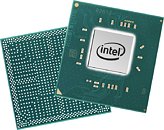
Intel "Elkhart Lake" is a Low-power SoC that Embeds Gen11 Graphics
The latest patches to Intel's open-source *nix drivers drop hints of a new low-power SoC in the works, codenamed "Elkhart Lake" featuring the company's most advanced integrated graphics solution. "Elkhart Lake" is a 10 nm SoC that combines a CPU complex based on the "Tremont" microarchitecture, with an iGPU based on the company's Gen11 architecture. Gen11 makes its debut with the company's 10 nm "Ice Lake" processors, promising big gains in graphics performance. Prototypes of a typical variant of Gen11 have been found to feature a compute throughput of 1 TFLOP/s, making them perform roughly on par with AMD's current "Raven Ridge" processors.
Source:
Intel GFX Patch

11 Comments on Intel "Elkhart Lake" is a Low-power SoC that Embeds Gen11 Graphics
Just a little rant on why Intel WON'T crush AMD APU's. AMD can still add more EU's themselves (especially with 7nm)! ;)
Vega 8 and 11 have 512:32:8 (8 CU) and 704:44:8 (11 CU) respectively. Vega 3 has 192:12:4 (3 CU).
The common UHD 630 (GT2) has 192:24:3 (24 EU), current iteration of Iris Plus (GT3e) is 655 with 384:48:6 (48 EU).
Iris Pro 580 (GT4e) exists with 576:72:9 (72 EU) on high-end mobile-ish Skylake chips but these are rare, as far as I remember Skull Canyon was the only one with it that got some traction.
Out of widely available parts, Vega 3 would be the best (but not perfect) comparison to UHD 630. Comparing these directly is complicated by the different CPUs these are attached to but when compared they are roughly on par - not exactly due to different focus in resource balance. Search for Athlon 200GE reviews, some of these have iGPU benchmark results.
Intel's iGPU performance is fairly appropriate to the amount of execution units (and clocks) they have. AMDs iGPUs are simply far larger at this point. There is an argument to be made about Intel's iGPU using more die space but probably no real way to have a definite answer to that.
Still, they've spared on screen, but at least they didn't cripple battery life and stay at 9+ hours, while most competitors manage to bring it down to 4.
As Intel APU will never cost much less than comparable AMD's, the only company that could suffer from Intel's iGPU buff is the greedy green.
I mean, is it me, or has anyone else noticed they're using stacking, b/c they literally can't make real chips on 10nm? Sure, it sounds nice and dandy for package size, but what it screams to me is that they want as small of dies as possible. And will probably use it anywhere possible (heat be damned no doubt). If 10nm didn't suck so bad, then there wouldn't be any reason to invest in stacking right now. The dies are already small. Or did they just not want to "glue" chiplets together right away and admit AMD did it right? I don't believe it's an economical solution.