Apr 22nd, 2025 03:38 EDT
change timezone
Latest GPU Drivers
New Forum Posts
- Yet another Case FAN topic and which Fans to choose (5)
- 5060 Ti 8GB DOA (116)
- What are you playing? (23415)
- am i alone to still using an asus p6t motherboard in the world ? (96)
- White Taichi 7900XTX (4)
- To distill or not distill what say ye? (34)
- Need thoughts on a quiet PC that's great for rendering, video editing and office work... (14)
- [Test Build] Fix for 576.02 Driver Install (44)
- Gainward Phoenix RTX 5070ti Temperatures (12)
- AAF Optimus Modded Driver For Windows 10 & Windows 11 - Only for Realtek HDAUDIO Chips (434)
Popular Reviews
- ASRock X870E Taichi Lite Review
- ASUS GeForce RTX 5060 Ti TUF OC 16 GB Review
- NVIDIA GeForce RTX 5060 Ti PCI-Express x8 Scaling
- Palit GeForce RTX 5060 Ti Infinity 3 16 GB Review
- MSI GeForce RTX 5060 Ti Gaming OC 16 GB Review
- Sapphire Radeon RX 9070 XT Pulse Review
- Upcoming Hardware Launches 2025 (Updated Apr 2025)
- Teevolution Terra Pro Review
- Sapphire Radeon RX 9070 XT Nitro+ Review - Beating NVIDIA
- ASUS GeForce RTX 5060 Ti Prime OC 16 GB Review
Controversial News Posts
- NVIDIA GeForce RTX 5060 Ti 16 GB SKU Likely Launching at $499, According to Supply Chain Leak (182)
- NVIDIA Sends MSRP Numbers to Partners: GeForce RTX 5060 Ti 8 GB at $379, RTX 5060 Ti 16 GB at $429 (127)
- NVIDIA Launches GeForce RTX 5060 Series, Beginning with RTX 5060 Ti This Week (115)
- Nintendo Confirms That Switch 2 Joy-Cons Will Not Utilize Hall Effect Stick Technology (105)
- Nintendo Switch 2 Launches June 5 at $449.99 with New Hardware and Games (99)
- Sony Increases the PS5 Pricing in EMEA and ANZ by Around 25 Percent (85)
- NVIDIA PhysX and Flow Made Fully Open-Source (77)
- Windows Notepad Gets Microsoft Copilot Integration (75)
News Posts matching #TDP
Return to Keyword Browsing
AMD's Navi 31 Might Clock to 3 GHz, Partner Cards Will be Able to Overclock
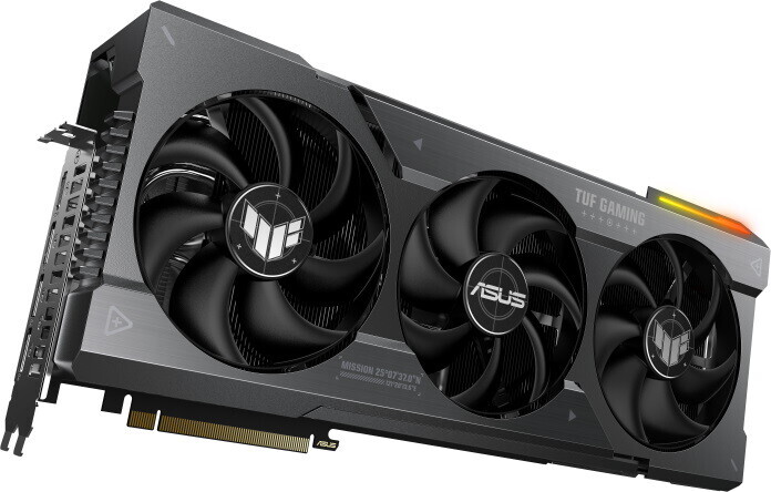
Based on details from a PCWorld livestream following AMD's launch of the Radeon RX 7000-series, it was revealed that AMD has designed the Navi 31 GPU to be able to scale as high as 3 GHz. In other words, it appears that AMD has power limited its cards, at least for the SKUs that the company has announced so far. This could be for many reasons, but most likely to try to find a balance between power and performance. The details of the 3 GHz scaling did however not come from AMD directly, but rather from Jarred Walton over at Tom's Hardware. That said, the information was apparently shared with the media by AMD at the event.
In the livestream, it was also confirmed that partner cards will be able to overclock, so expect to see some factory overclocked cards, with higher power draw. This could be why, in part, that ASUS went with a much larger cooler on its TUF Gaming Radeon RX 7900-series cards. As ASUS didn't reveal any clock speeds or TDPs of its two cards, we don't really know what to expect, but we'd be surprised if these cards weren't factory overclocked to some degree when they launch in December.
In the livestream, it was also confirmed that partner cards will be able to overclock, so expect to see some factory overclocked cards, with higher power draw. This could be why, in part, that ASUS went with a much larger cooler on its TUF Gaming Radeon RX 7900-series cards. As ASUS didn't reveal any clock speeds or TDPs of its two cards, we don't really know what to expect, but we'd be surprised if these cards weren't factory overclocked to some degree when they launch in December.

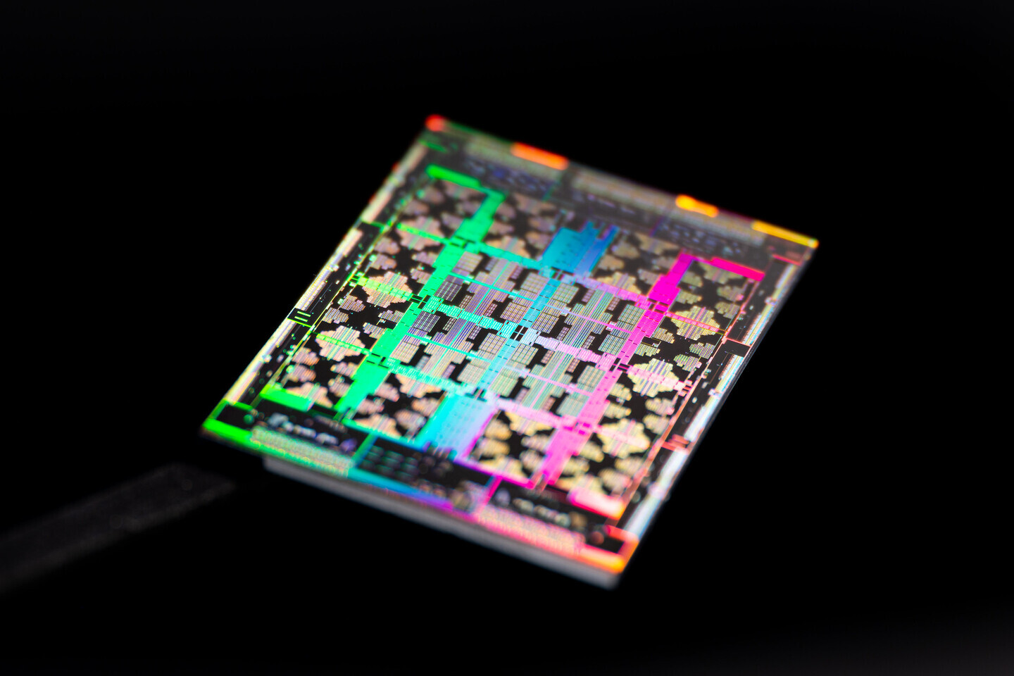
48-Core Russian Baikal-S Processor Die Shots Appear
In December of 2021, we covered the appearance of Russia's home-grown Baikal-S processor, which has 48 cores based on Arm Cortex-A75 cores. Today, thanks to the famous chip photographer Fritzchens Fritz, we have the first die shows that show us exactly how Baikal-S SoC is structured internally and what it is made up of. Manufactured on TSMC's 16 nm process, the Baikal-S BE-S1000 design features 48 Arm Cortex-A75 cores running at a 2.0 GHz base and a 2.5 GHz boost frequency. With a TDP of 120 Watts, the design seems efficient, and the Russian company promises performance comparable to Intel Skylake Xeons or Zen1-based AMD EPYC processors. It also uses a home-grown RISC-V core for management and controlling secure boot sequences.
Below, you can see the die shots taken by Fritzchens Fritz and annotated details by Twitter user Locuza that marked the entire SoC. Besides the core clusters, we see that a slum of cache connects everything, with six 72-bit DDR4-3200 PHYs and memory controllers surrounding everything. This model features a pretty good selection of I/O for a server CPU, as there are five PCIe 4.0 x16 (4x4) interfaces, with three supporting CCIX 1.0. You can check out more pictures below and see the annotations for yourself.


Below, you can see the die shots taken by Fritzchens Fritz and annotated details by Twitter user Locuza that marked the entire SoC. Besides the core clusters, we see that a slum of cache connects everything, with six 72-bit DDR4-3200 PHYs and memory controllers surrounding everything. This model features a pretty good selection of I/O for a server CPU, as there are five PCIe 4.0 x16 (4x4) interfaces, with three supporting CCIX 1.0. You can check out more pictures below and see the annotations for yourself.


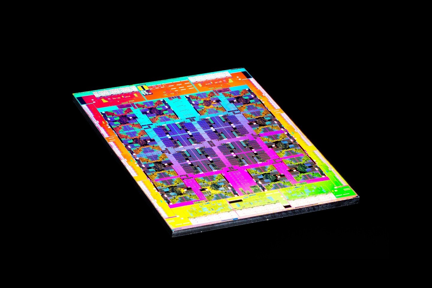


NVIDIA Introduces L40 Omniverse Graphics Card
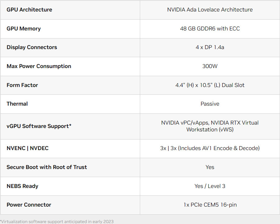
During its GTC 2022 session, NVIDIA introduced its new generation of gaming graphics cards based on the novel Ada Lovelace architecture. Dubbed NVIDIA GeForce RTX 40 series, it brings various updates like more CUDA cores, a new DLSS 3 version, 4th generation Tensor cores, 3rd generation Ray Tracing cores, and much more, which you can read about here. However, today, we also got a new Ada Lovelace card intended for the data center. Called the L40, NVIDIA updated its previous Ampere-based A40 design. While the NVIDIA website provides sparse, the new L40 GPU uses 48 GB GDDR6 memory with ECC error correction. Using NVLink, you can get 96GBs of VRAM. Paired with an unknown SKU, we assume that it uses AD102 with adjusted frequencies to lower the TDP and allow for passive cooling.
NVIDIA is calling this their Omniverse GPU, as it is a part of the push to separate its GPUs used for graphics and AI/HPC models. The "L" model in the current product stack is used to accelerate graphics, with display ports installed on the GPU, while the "H" models (H100) are there to accelerate HPC/AI installments where visual elements are a secondary task. This is a further separation of the entire GPU market, where the HPC/AI SKUs get their own architecture, and GPUs for graphics processing are built on a new architecture as well. You can see the specifications provided by NVIDIA below.
NVIDIA is calling this their Omniverse GPU, as it is a part of the push to separate its GPUs used for graphics and AI/HPC models. The "L" model in the current product stack is used to accelerate graphics, with display ports installed on the GPU, while the "H" models (H100) are there to accelerate HPC/AI installments where visual elements are a secondary task. This is a further separation of the entire GPU market, where the HPC/AI SKUs get their own architecture, and GPUs for graphics processing are built on a new architecture as well. You can see the specifications provided by NVIDIA below.
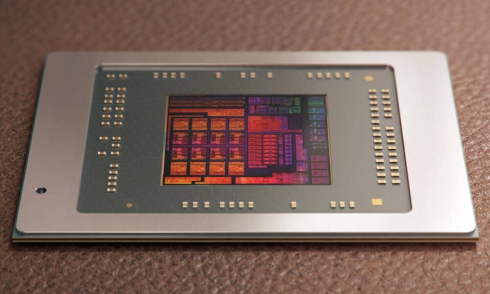
AMD Ryzen 7000 Undervolting Yields Great Results with Temperatures
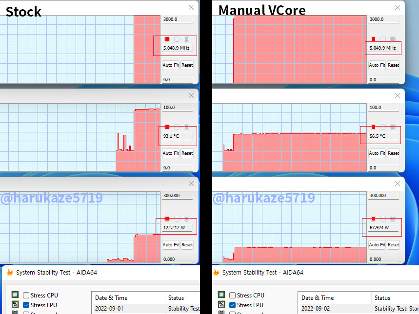
AMD Ryzen 7000 "Zen 4" processors can hit up to 95 °C at stock settings, with cooling most appropriate to the TDP level. This is because the PPT (package power tracking) limits for the 170 W TDP processors is as high as 230 W, and for the 105 W TDP models, it's 130 W. After reaching this temperature threshold, the processor begins to downclock itself to lower temperatures. Harukaze5719 discovered that higher than needed core voltages could be at play, and manually undervolting the processors could free up significant thermal headroom, letting the processors hold on to higher boost multipliers better.

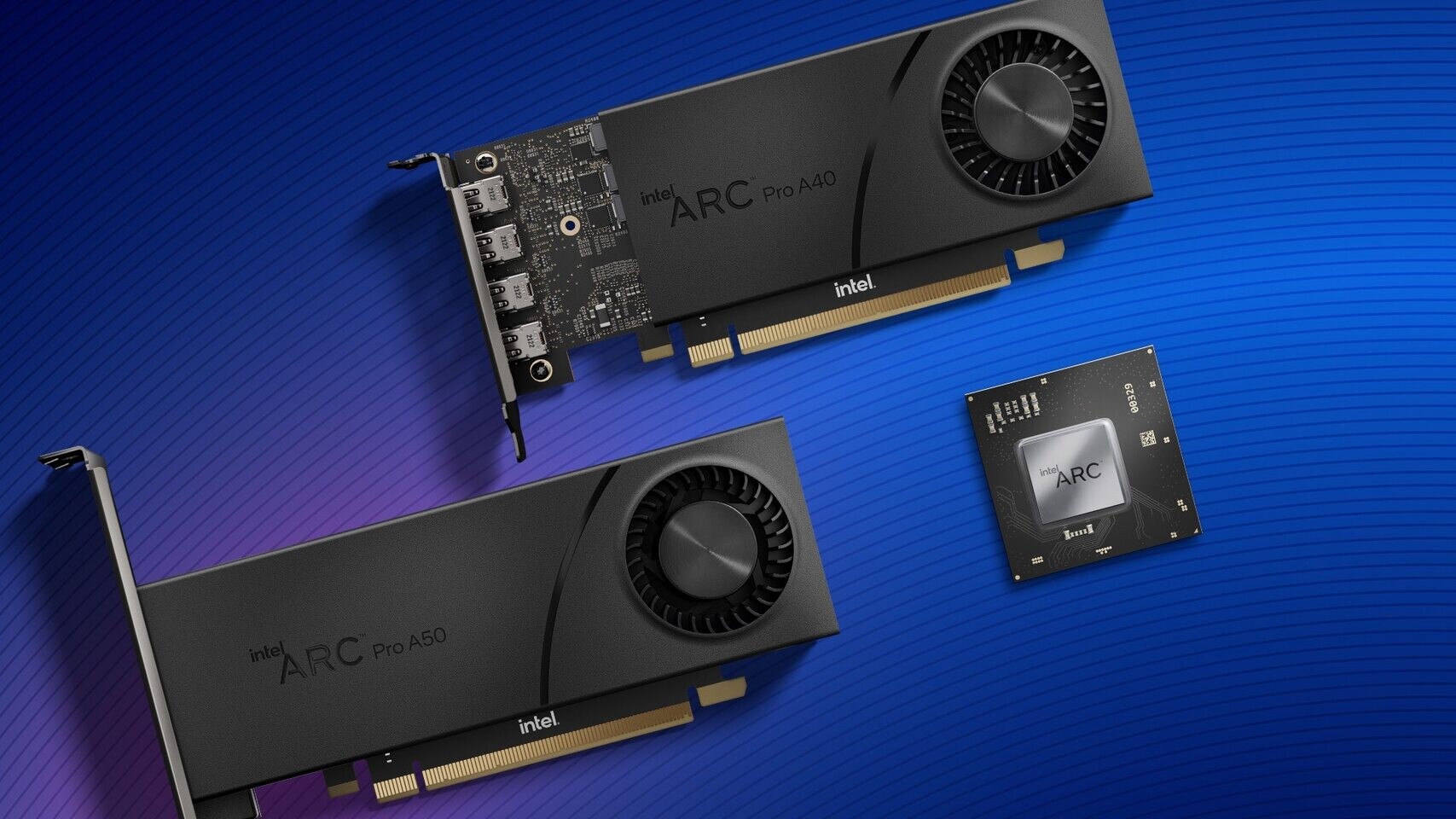
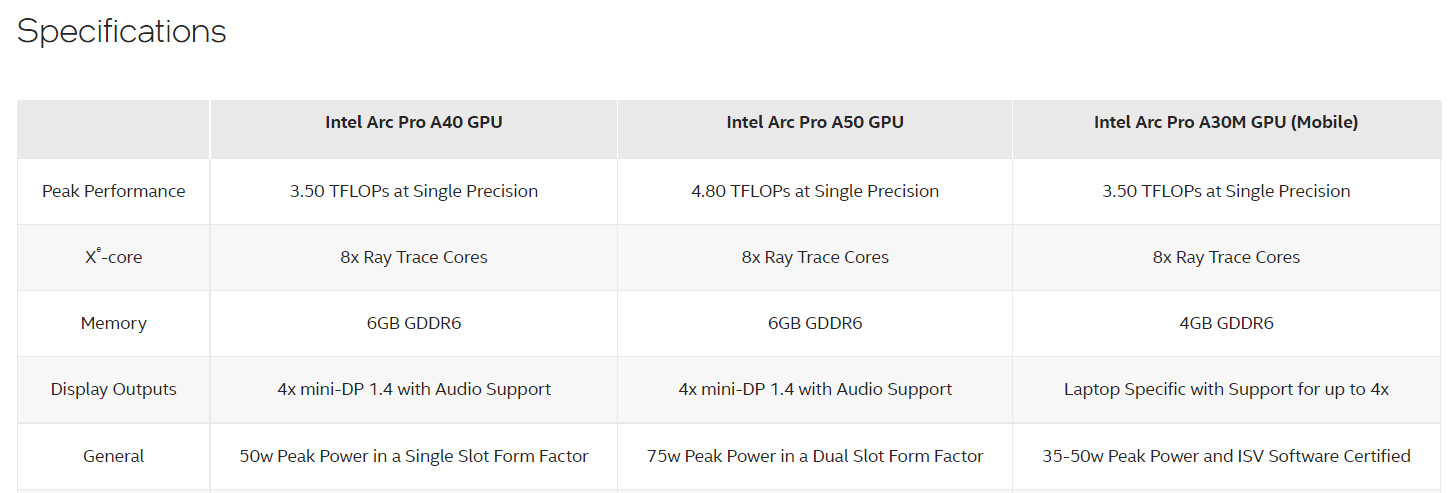
Intel Unveils Arc Pro Graphics Cards for Workstations and Professional Software
Intel has today unveiled another addition to its discrete Arc Alchemist graphics card lineup, with a slight preference to the professional consumer market. Intel has prepared three models for creators and entry pro-vis solutions, called Intel Arc Pro graphics cards. All GPUs are AV1 accelerated, have ray tracing support, and are designed to handle AI acceleration inside applications like Adobe Premiere Pro. At the start, we have a small A30M mobile GPU aimed at laptop designs. It has a 3.5 TeraFLOP FP32 capability inside a configurable 35-50 Watt TDP envelope, has eight ray tracing cores, and 4 GB of GDDR6 memory. Its display output connectors depend on OEM's laptop design.
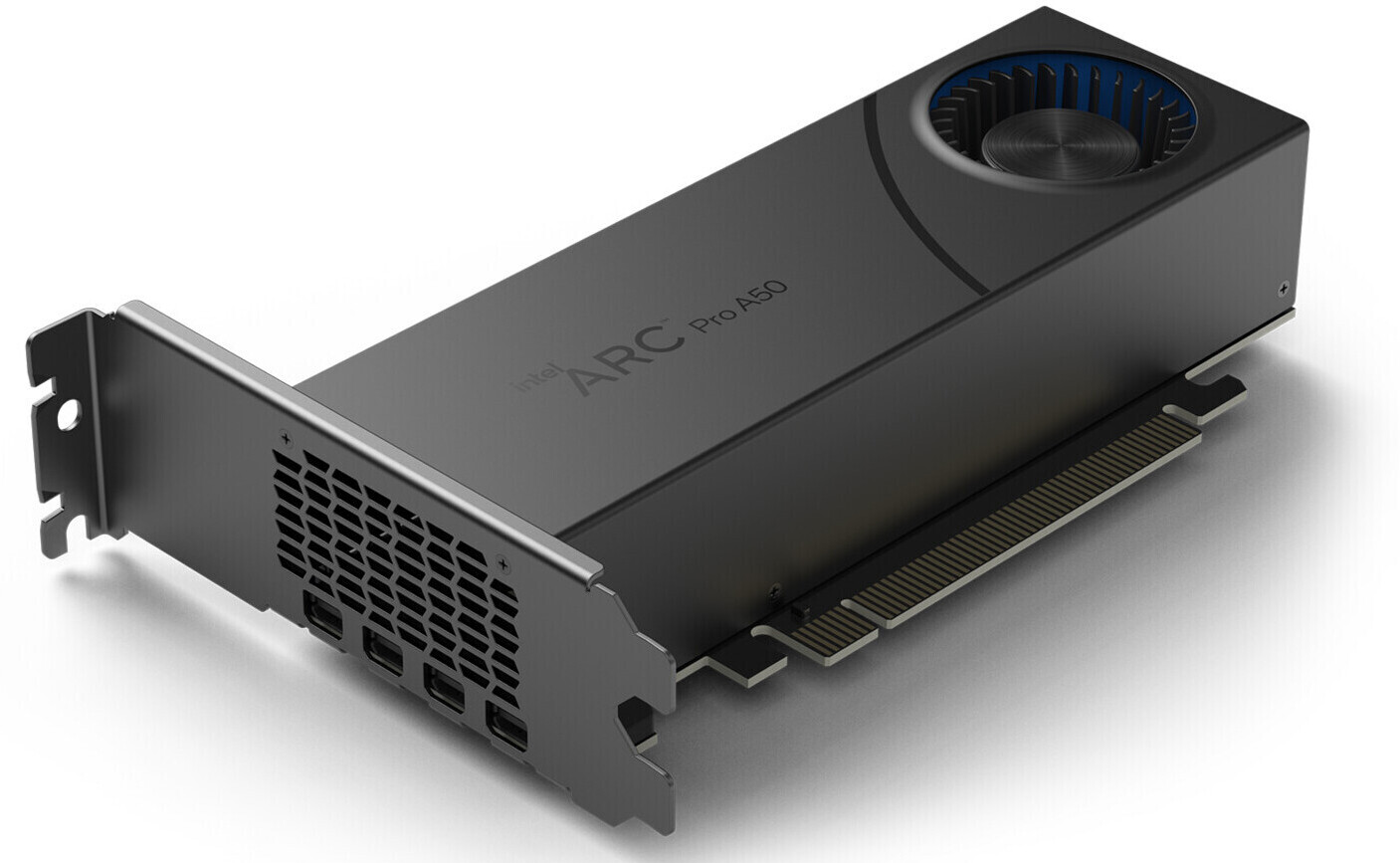
Next, we have the Arc A40 Pro discrete single-slot GPU. Having 3.5 TeraFLOPs of FP32 single-precision performance, it has eight ray tracing cores and 6 GB of GDDR6 memory. The listed maximum TDP for this model is 50 Watts. It has four mini-DP ports for video output, and it can drive two monitors at 8K 60 Hz, one at 5K 240 Hz, two at 5K 120 Hz, or four at 4K 60 Hz refresh rate. Its bigger brother, the Arc A50 Pro, is a dual-slot design with 4.8 TeraFLOPs of single-precision FP32 computing, has eight ray tracing cores, and 6 GB of GDDR6 memory as well. It has the same video output capability as the Arc A40 Pro, with a beefier cooling setup to handle the 75 Watt TDP. All software developed using the OneAPI toolkit can be accelerated using these GPUs. Intel is working with the industry to adapt professional software for Arc Pro graphics.


Next, we have the Arc A40 Pro discrete single-slot GPU. Having 3.5 TeraFLOPs of FP32 single-precision performance, it has eight ray tracing cores and 6 GB of GDDR6 memory. The listed maximum TDP for this model is 50 Watts. It has four mini-DP ports for video output, and it can drive two monitors at 8K 60 Hz, one at 5K 240 Hz, two at 5K 120 Hz, or four at 4K 60 Hz refresh rate. Its bigger brother, the Arc A50 Pro, is a dual-slot design with 4.8 TeraFLOPs of single-precision FP32 computing, has eight ray tracing cores, and 6 GB of GDDR6 memory as well. It has the same video output capability as the Arc A40 Pro, with a beefier cooling setup to handle the 75 Watt TDP. All software developed using the OneAPI toolkit can be accelerated using these GPUs. Intel is working with the industry to adapt professional software for Arc Pro graphics.

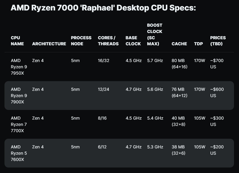
Potential Ryzen 7000-series CPU Specs and Pricing Leak, Ryzen 9 7950X Expected to hit 5.7 GHz
It's pretty clear that we're getting very close to the launch of AMD's AM5 platform and the Ryzen 7000-series CPUs, with spec details and even pricing brackets tipping up online. Wccftech has posted what the publication believes will be the lineup we can expect to launch in just over a month's time, if rumours are to be believed. The base model is said to be the Ryzen 5 7600X, which the site claims will have a base clock of 4.7 GHz and a boost clock of 5.3 GHz. There's no change in processor core or thread count compared to the current Ryzen 5 5600X, but the L2 cache appears to have doubled, for a total of 38 MB of cache. This is followed by the Ryzen 7 7700X, which starts out a tad slower with a base clock of 4.5 GHz, but it has a slightly higher boost clock of 5.4 GHz. Likewise here, the core and thread count remains unchanged, while the L2 cache also gets a bump here for a total of 40 MB cache. Both these models are said to have a 105 W TDP.
The Ryzen 9 7900X is said to have a 4.7 GHz base clock and a 5.6 GHz boost clock, so a 200 MHz jump up from the Ryzen 7 7700X. This CPU has a total of 76 MB of cache. Finally the Ryzen 9 7950X is said to have the same base clock of 4.5 GHz as the Ryzen 7 7700X, but it has the highest boost clock of all the expected models at 5.7 GHz, while having a total of 80 MB cache. These two SKUs are both said to have a 170 W TDP. Price wise, from top to bottom, we might be looking at somewhere around US$700, US$600, US$300 and US$200, so it seems like AMD has adjusted its pricing downwards by around $100 on the low-end, with the Ryzen 7 part fitting the same price bracket as the Ryzen 7 5700X. The Ryzen 9 7900X seems to have had its price adjusted upwards slightly, while the Ryzen 9 7950X seems to be expected to be priced lower than its predecessors. Take these things with the right helping of scepticism for now, as things can still change before the launch.
The Ryzen 9 7900X is said to have a 4.7 GHz base clock and a 5.6 GHz boost clock, so a 200 MHz jump up from the Ryzen 7 7700X. This CPU has a total of 76 MB of cache. Finally the Ryzen 9 7950X is said to have the same base clock of 4.5 GHz as the Ryzen 7 7700X, but it has the highest boost clock of all the expected models at 5.7 GHz, while having a total of 80 MB cache. These two SKUs are both said to have a 170 W TDP. Price wise, from top to bottom, we might be looking at somewhere around US$700, US$600, US$300 and US$200, so it seems like AMD has adjusted its pricing downwards by around $100 on the low-end, with the Ryzen 7 part fitting the same price bracket as the Ryzen 7 5700X. The Ryzen 9 7900X seems to have had its price adjusted upwards slightly, while the Ryzen 9 7950X seems to be expected to be priced lower than its predecessors. Take these things with the right helping of scepticism for now, as things can still change before the launch.
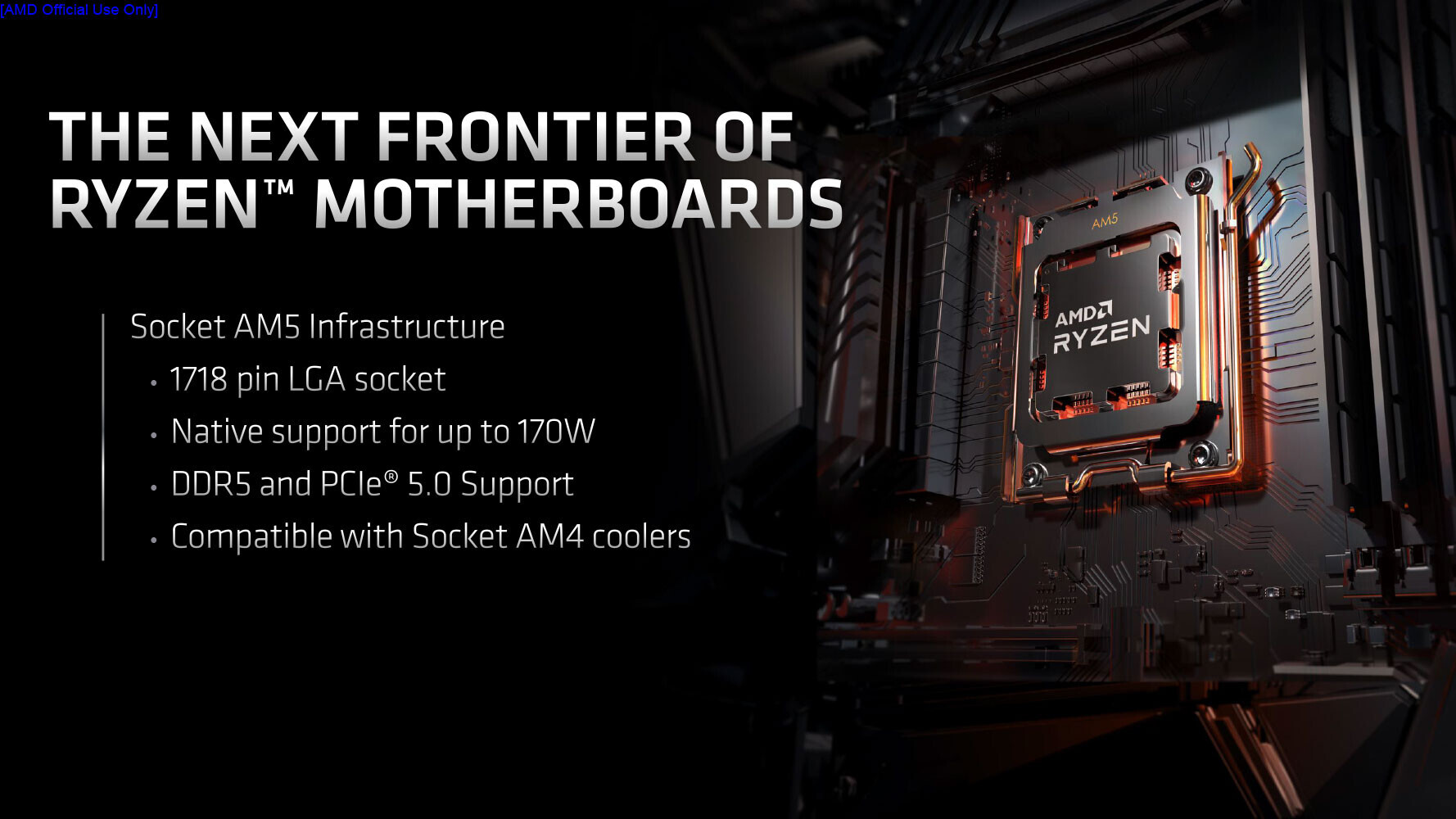
AMD Clarifies Ryzen 7000 "Zen 4" TDP and Power Limits: 170W TDP, 230W PPT
The mention of "170 W" in one of the slides of AMD's Computex 2022 reveal of the upcoming Ryzen 7000 "Zen 4" desktop processors, caused quite some confusion as to what that figure meant. AMD issued a structured clarification on the matter, laying to rest the terminology associated with it. Apparently, there will be certain SKUs of Socket AM5 processors with TDP of 170 W. This would be the same classical definition of TDP that AMD has been consistently using. The package-power tracking (PPT), a figure that translates as power limit for the socket, is 230 W.
This does not necessarily mean that there will be a Ryzen 7000-series SKU with 170 W TDP. AMD plans to give AM5 a similar life-cycle to AM4, which is now spanning five generations of Ryzen processors, and the 170 W TDP and 230 W PPT figures only denote design goals for the socket. AMD, in a statement, explained why it needed to make AM5 capable of delivering much higher power than AM4 could—to enable higher CPU core-counts in the future, more on-package hardware, and for new capabilities like power-hungry instruction-sets (think AVX-512). AMD has been calculating PPT as 1.35 times TDP, since the very first generation of Ryzen chips. For a 105 W TDP processor, this means 140 W PPT, and the same formula continues with Ryzen 7000 series (230 W is 1.35x 170 W). The AMD statement follows.
This does not necessarily mean that there will be a Ryzen 7000-series SKU with 170 W TDP. AMD plans to give AM5 a similar life-cycle to AM4, which is now spanning five generations of Ryzen processors, and the 170 W TDP and 230 W PPT figures only denote design goals for the socket. AMD, in a statement, explained why it needed to make AM5 capable of delivering much higher power than AM4 could—to enable higher CPU core-counts in the future, more on-package hardware, and for new capabilities like power-hungry instruction-sets (think AVX-512). AMD has been calculating PPT as 1.35 times TDP, since the very first generation of Ryzen chips. For a 105 W TDP processor, this means 140 W PPT, and the same formula continues with Ryzen 7000 series (230 W is 1.35x 170 W).
Russia to Use Chinese Zhaoxin x86 Processors Amidst Restrictions to Replace Intel and AMD Designs
Many companies, including Intel and AMD, have stopped product shipments to Russia amidst the war in Ukraine in the past few months. This has left the Russian state without any new processors from the two prominent x86 designers, thus slowing down the country's technological progress. To overcome this issue, it seems like the solution is embedded in the Chinese Zhaoxin x86 CPUs. According to the latest report from Habr, a motherboard designer called Dannie is embedding Chinese Zhaoxin x86 CPUs into motherboards to provide the motherland with an x86-capable processor. More precisely, the company had designed a BX-Z60A micro-ATX motherboard that embeds Zhaoxin's KaiXian KX-6640MA SoC with eight cores based on LuJiaZui microarchitecture. The SoC is clocked at a frequency range of 2.1-2.7 GHz, carries 4 MB of L2 cache, 16 lanes of PCIe 3.0, and has integrated graphics, all in a 25 Watt TDP.
As far as the motherboard is concerned, it supports two DDR4 memory slots, two PCIe x16 connectors, M.2-2280 and M.2-2230 slots, and three SATA III connectors for storage. For I/O you have USB ports, DisplayPort, HDMI, VGA/D-Sub, GbE, 3.5-mm audio, and additional PS/2 ports. This is a pretty decent selection; however, we don't know the pricing structure. A motherboard with KaiXian KX-6640MA SoC like this is certainly not cheap, so we are left to wonder if this will help Russian users deal with the newly imposed restriction on importing US tech.

As far as the motherboard is concerned, it supports two DDR4 memory slots, two PCIe x16 connectors, M.2-2280 and M.2-2230 slots, and three SATA III connectors for storage. For I/O you have USB ports, DisplayPort, HDMI, VGA/D-Sub, GbE, 3.5-mm audio, and additional PS/2 ports. This is a pretty decent selection; however, we don't know the pricing structure. A motherboard with KaiXian KX-6640MA SoC like this is certainly not cheap, so we are left to wonder if this will help Russian users deal with the newly imposed restriction on importing US tech.

NVIDIA GeForce RTX 4090 Twice as Fast as RTX 3090, Features 16128 CUDA Cores and 450W TDP
NVIDIA's next-generation GeForce RTX 40 series of graphics cards, codenamed Ada Lovelace, is shaping up to be a powerful graphics card lineup. Allegedly, we can expect to see a mid-July launch of NVIDIA's newest gaming offerings, where customers can expect some impressive performance. According to a reliable hardware leaker, kopite7kimi, NVIDIA GeForce RTX 4090 graphics card will feature AD102-300 GPU SKU. This model is equipped with 126 Streaming Multiprocessors (SMs), which brings the total number of FP32 CUDA cores to 16128. Compared to the full AD102 GPU with 144 SMs, this leads us to think that there will be an RTX 4090 Ti model following up later as well.
Paired with 24 GB of 21 Gbps GDDR6X memory, the RTX 4090 graphics card has a TDP of 450 Watts. While this number may appear as a very power-hungry design, bear in mind that the targeted performance improvement over the previous RTX 3090 model is expected to be a two-fold scale. Paired with TSMC's new N4 node and new architecture design, performance scaling should follow at the cost of higher TDPs. These claims are yet to be validated by real-world benchmarks of independent tech media, so please take all of this information with a grain of salt and wait for TechPowerUp reviews once the card arrives.
Paired with 24 GB of 21 Gbps GDDR6X memory, the RTX 4090 graphics card has a TDP of 450 Watts. While this number may appear as a very power-hungry design, bear in mind that the targeted performance improvement over the previous RTX 3090 model is expected to be a two-fold scale. Paired with TSMC's new N4 node and new architecture design, performance scaling should follow at the cost of higher TDPs. These claims are yet to be validated by real-world benchmarks of independent tech media, so please take all of this information with a grain of salt and wait for TechPowerUp reviews once the card arrives.
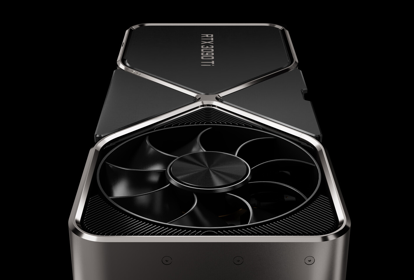
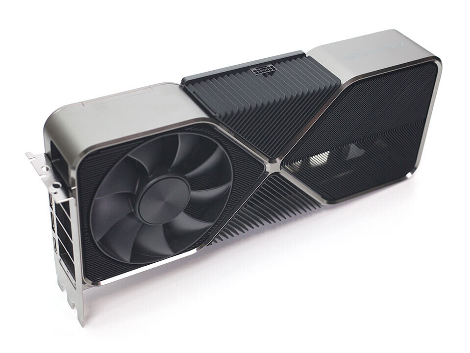
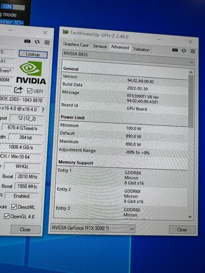
NVIDIA GeForce RTX 3090 Ti Gets Custom 890 Watt XOC BIOS
Extreme overclocking is an enthusiast discipline where overclockers try to push their hardware to extreme limits. Combining powerful cooling solutions like liquid nitrogen (LN2), which reaches sub-zero temperatures alongside modified hardware, the silicon can output tremendous power. Today, we are witnessing a custom XOC (eXtreme OverClocking) BIOS for the NVIDIA GeForce RTX 3090 Ti graphics card that can push the GA102 SKU to impressive 890 Watts of power, representing almost a two-fold increase to the stock TDP. Enthusiasts pursuing large frequencies with their RTX 3090 Ti are likely users of this XOC BIOS. However, most likely, we will see GALAX HOF or EVGA KINGPIN cards with dual 16-pin power connectors utilize this.
As shown below, MEGAsizeGPU, the creator of this BIOS, managed to push his ASUS GeForce RTX 3090 Ti TUF with XOC BIOS to 615 Watts, so KINGPIN and HOF designs will have to be used to draw all the possible heat. The XOC BIOS was uploaded to our VGA BIOS database, however, caution is advised as this can break your graphics card.

As shown below, MEGAsizeGPU, the creator of this BIOS, managed to push his ASUS GeForce RTX 3090 Ti TUF with XOC BIOS to 615 Watts, so KINGPIN and HOF designs will have to be used to draw all the possible heat. The XOC BIOS was uploaded to our VGA BIOS database, however, caution is advised as this can break your graphics card.
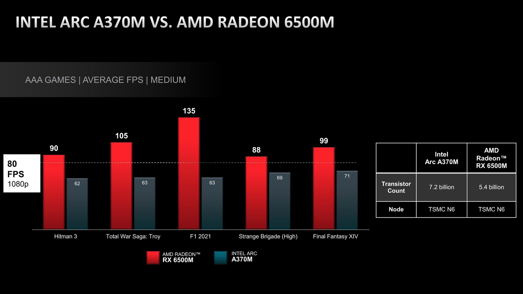
AMD Claims Radeon RX 6500M is Faster Than Intel Arc A370M Graphics
A few days ago, Intel announced its first official discrete graphics card efforts, designed for laptops. Called the Arc Alchemist lineup, Intel has designed these SKUs to provide entry-level to high-end options covering a wide range of use cases. Today, AMD has responded with a rather exciting Tweet made by the company's @Radeon Twitter account. The company compared Intel's Arc Alchemist A370M GPU with AMD's Radeon RX 6500M mobile SKUs in the post. These GPUs are made on TSMC's N6 node, feature 4 GB GDDR6 64-bit memory, 1024 FP32 cores, and have the same configurable TDP range of 35-50 Watts.
Below, you can see AMD's benchmarks of the following select games: Hitman 3, Total War Saga: Troy, F1 2021, Strange Brigade (High), and Final Fantasy XIV. The Radeon RX 6500M GPU manages to win in all of these games, thus explaining AMD's "FTW" hashtag on Twitter. Remember that these are vendor-supplied benchmarks runs, so we have to wait for some media results to surface.
Below, you can see AMD's benchmarks of the following select games: Hitman 3, Total War Saga: Troy, F1 2021, Strange Brigade (High), and Final Fantasy XIV. The Radeon RX 6500M GPU manages to win in all of these games, thus explaining AMD's "FTW" hashtag on Twitter. Remember that these are vendor-supplied benchmarks runs, so we have to wait for some media results to surface.
AMD Ryzen 7000 Series "Raphael" Processors to Come with up to 170 Watt TDP for 16-Core SKUs
AMD is slowly preparing to transition its consumer base into a new platform and processor architecture with the launch of Ryzen 7000 series processors codenamed Raphael. Based on the new AM5 LGA socket, these processors will come with up to 16 cores and 32 threads at the top-end configurations. Thanks to the latest round of rumors, we managed to find out just what TDP rating two SKUs will carry. According to a well-known leaker @graymon55, AMD is rating the 12-core SKU with a TDP of 105 Watts. On the other hand, the top-end 16-core 7000 series SKU replacing the current Ryzen 9 5950X will carry a large TDP of 170 Watts.
The 170 Watt TDP configuration will likely require better cooling efforts. AMD will probably advise users to invest in better cooling solutions, such as AIO liquid coolers or giant air coolers.
The 170 Watt TDP configuration will likely require better cooling efforts. AMD will probably advise users to invest in better cooling solutions, such as AIO liquid coolers or giant air coolers.
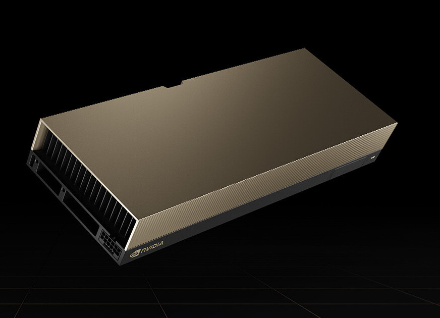
NVIDIA H100 is a Compute Monster with 80 Billion Transistors, New Compute Units and HBM3 Memory
During the GTC 2022 keynote, NVIDIA announced its newest addition to the accelerator cards family. Called NVIDIA H100 accelerator, it is the company's most powerful creation ever. Utilizing 80 billion of TSMC's 4N 4 nm transistors, H100 can output some insane performance, according to NVIDIA. Featuring a new fourth-generation Tensor Core design, it can deliver a six-fold performance increase compared to A100 Tensor Cores and a two-fold MMA (Matrix Multiply Accumulate) improvement. Additionally, new DPX instructions accelerate Dynamic Programming algorithms up to seven times over the previous A100 accelerator. Thanks to the new Hopper architecture, the Streaming Module structure has been optimized for better transfer of large data blocks.
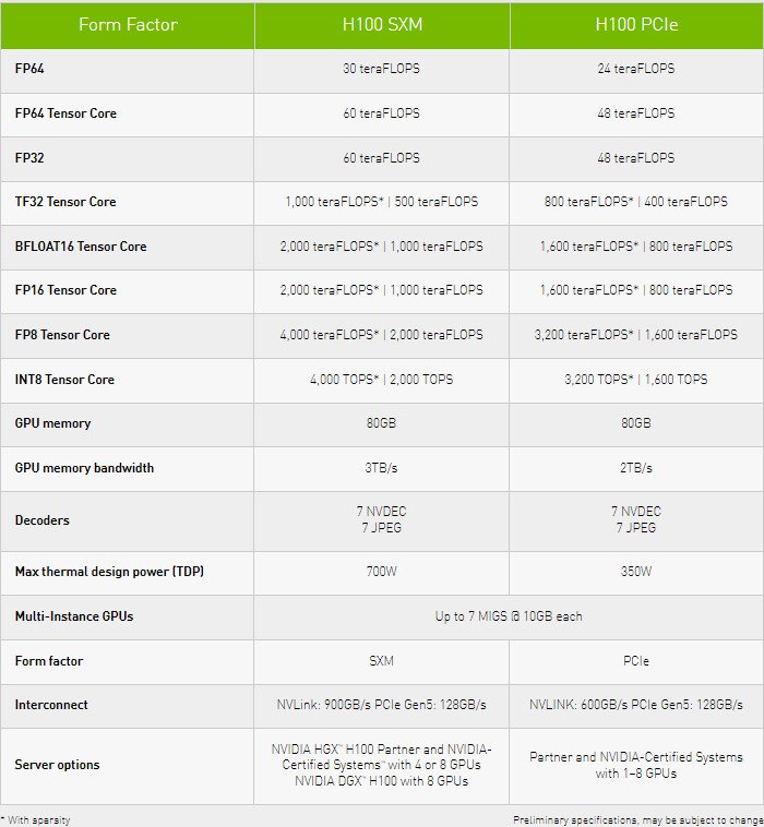
The full GH100 chip implementation features 144 SMs, and 128 FP32 CUDA cores per SM, resulting in 18,432 CUDA cores at maximum configuration. The NVIDIA H100 GPU with SXM5 board form-factor features 132 SMs, totaling 16,896 CUDA cores, while the PCIe 5.0 add-in card has 114 SMs, totaling 14,592 CUDA cores. As much as 80 GB of HBM3 memory surrounds the GPU at 3 TB/s bandwidth. Interestingly, the SXM5 variant features a very large TDP of 700 Watts, while the PCIe card is limited to 350 Watts. This is the result of better cooling solutions offered for the SXM form-factor. As far as performance figures are concerned, the SXM and PCIe versions provide two distinctive figures for each implementation. You can check out the performance estimates in various precision modes below. You can read more about the Hopper architecture and what makes it special in this whitepaper published by NVIDIA.

The full GH100 chip implementation features 144 SMs, and 128 FP32 CUDA cores per SM, resulting in 18,432 CUDA cores at maximum configuration. The NVIDIA H100 GPU with SXM5 board form-factor features 132 SMs, totaling 16,896 CUDA cores, while the PCIe 5.0 add-in card has 114 SMs, totaling 14,592 CUDA cores. As much as 80 GB of HBM3 memory surrounds the GPU at 3 TB/s bandwidth. Interestingly, the SXM5 variant features a very large TDP of 700 Watts, while the PCIe card is limited to 350 Watts. This is the result of better cooling solutions offered for the SXM form-factor. As far as performance figures are concerned, the SXM and PCIe versions provide two distinctive figures for each implementation. You can check out the performance estimates in various precision modes below. You can read more about the Hopper architecture and what makes it special in this whitepaper published by NVIDIA.

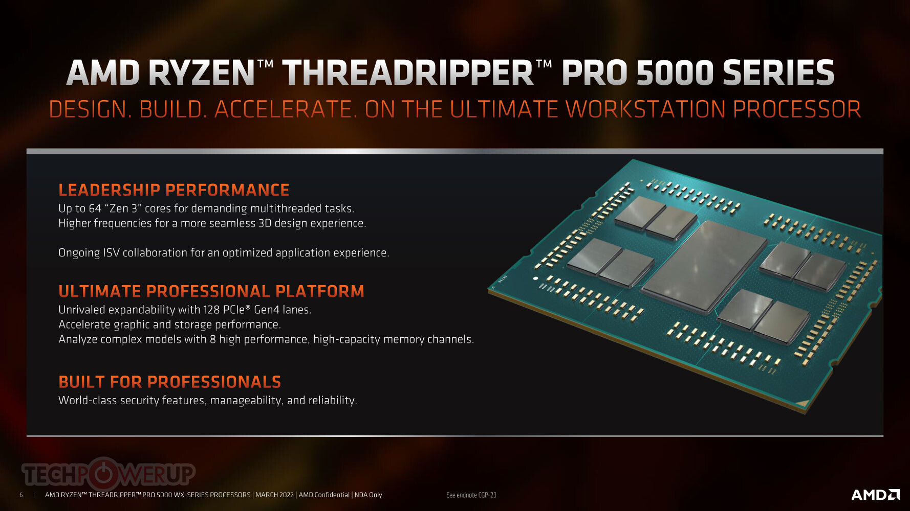
AMD Announces Zen 3 Threadripper 5000, but only for Professionals
AMD today launched its first Ryzen Threadripper processors based on the "Zen 3" microarchitecture, with the Ryzen Threadripper PRO 5000WX series. Designed to be drop-in compatible with workstations and motherboards based on the AMD WRX80 chipset, these processors come in core-counts of up to 64-core/128-thread, with an enormous I/O offering that includes 8-channel DDR4 memory with ECC support, and a 128-lane PCI-Express 4.0 root complex. The biggest change over the previous generation Threadripper PRO 3000WX series has to be the use of "Zen 3" CCDs, each with 8 CPU cores, sharing a common 32 MB of L3 cache. AMD isn't using the "Zen 3" chiplets with 3DV Cache.
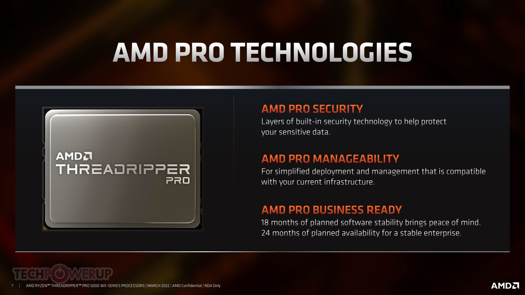
The full AMD PRO management feature-set from Ryzen PRO is available on these processors, including PRO Security, PRO Management, and a special support channel that includes planned parts and software availability. What's more, AMD has been working with ISVs of most professional content-creation software since the past generation of Ryzen Threadripper PRO, to optimize their software for the processors (high core-counts, NUMA topology, etc.). The benefits of these are shared with all generations of Threadrippers. Although all parts in the Threadripper PRO 5000WX series are rated for a TDP of 280 W, AMD claims to have worked on power-management, offering up to 67 percent lower power per core, compared to the competition (2P Xeon Scalable Platinum 8280).


The full AMD PRO management feature-set from Ryzen PRO is available on these processors, including PRO Security, PRO Management, and a special support channel that includes planned parts and software availability. What's more, AMD has been working with ISVs of most professional content-creation software since the past generation of Ryzen Threadripper PRO, to optimize their software for the processors (high core-counts, NUMA topology, etc.). The benefits of these are shared with all generations of Threadrippers. Although all parts in the Threadripper PRO 5000WX series are rated for a TDP of 280 W, AMD claims to have worked on power-management, offering up to 67 percent lower power per core, compared to the competition (2P Xeon Scalable Platinum 8280).


Intel Details Ponte Vecchio Accelerator: 63 Tiles, 600 Watt TDP, and Lots of Bandwidth
During the International Solid-State Circuits Conference (ISSCC) 2022, Intel gave us a more significant look at its upcoming Ponte Vecchio HPC accelerator and how it operates. So far, Intel convinced us that the company created Ponte Vecchio out of 47 tiles glued together in one package. However, the ISSCC presentation shows that the accelerator is structured rather interestingly. There are 63 tiles in total, where 16 are reserved for compute, eight are used for RAMBO cache, two are Foveros base tiles, two represent Xe-Link tiles, eight are HBM2E tiles, and EMIB connection takes up 11 tiles. This totals for about 47 tiles. However, an additional 16 thermal tiles used in Ponte Vecchio regulate the massive TDP output of this accelerator.
What is interesting is that Intel gave away details of the RAMBO cache. This novel SRAM technology uses four banks of 3.75 MB groups total of 15 MB per tile. They are connected to the fabric at 1.3 TB/s connection per chip. In contrast, compute tiles are connected at 2.6 TB/s speeds to the chip fabric. With eight RAMBO cache tiles, we get an additional 120 MB SRAM present. The base tile is a 646 mm² die manufactured in Intel 7 semiconductor process and contains 17 layers. It includes a memory controller, the Fully Integrated Voltage Regulators (FIVR), power management, 16-lane PCIe 5.0 connection, and CXL interface. The entire area of Ponte Vecchio is rather impressive, as 47 active tiles take up 2,330 mm², whereas when we include thermal dies, the total area jumps to 3,100 mm². And, of course, the entire package is much larger at 4,844 mm², connected to the system with 4,468 pins.


What is interesting is that Intel gave away details of the RAMBO cache. This novel SRAM technology uses four banks of 3.75 MB groups total of 15 MB per tile. They are connected to the fabric at 1.3 TB/s connection per chip. In contrast, compute tiles are connected at 2.6 TB/s speeds to the chip fabric. With eight RAMBO cache tiles, we get an additional 120 MB SRAM present. The base tile is a 646 mm² die manufactured in Intel 7 semiconductor process and contains 17 layers. It includes a memory controller, the Fully Integrated Voltage Regulators (FIVR), power management, 16-lane PCIe 5.0 connection, and CXL interface. The entire area of Ponte Vecchio is rather impressive, as 47 active tiles take up 2,330 mm², whereas when we include thermal dies, the total area jumps to 3,100 mm². And, of course, the entire package is much larger at 4,844 mm², connected to the system with 4,468 pins.


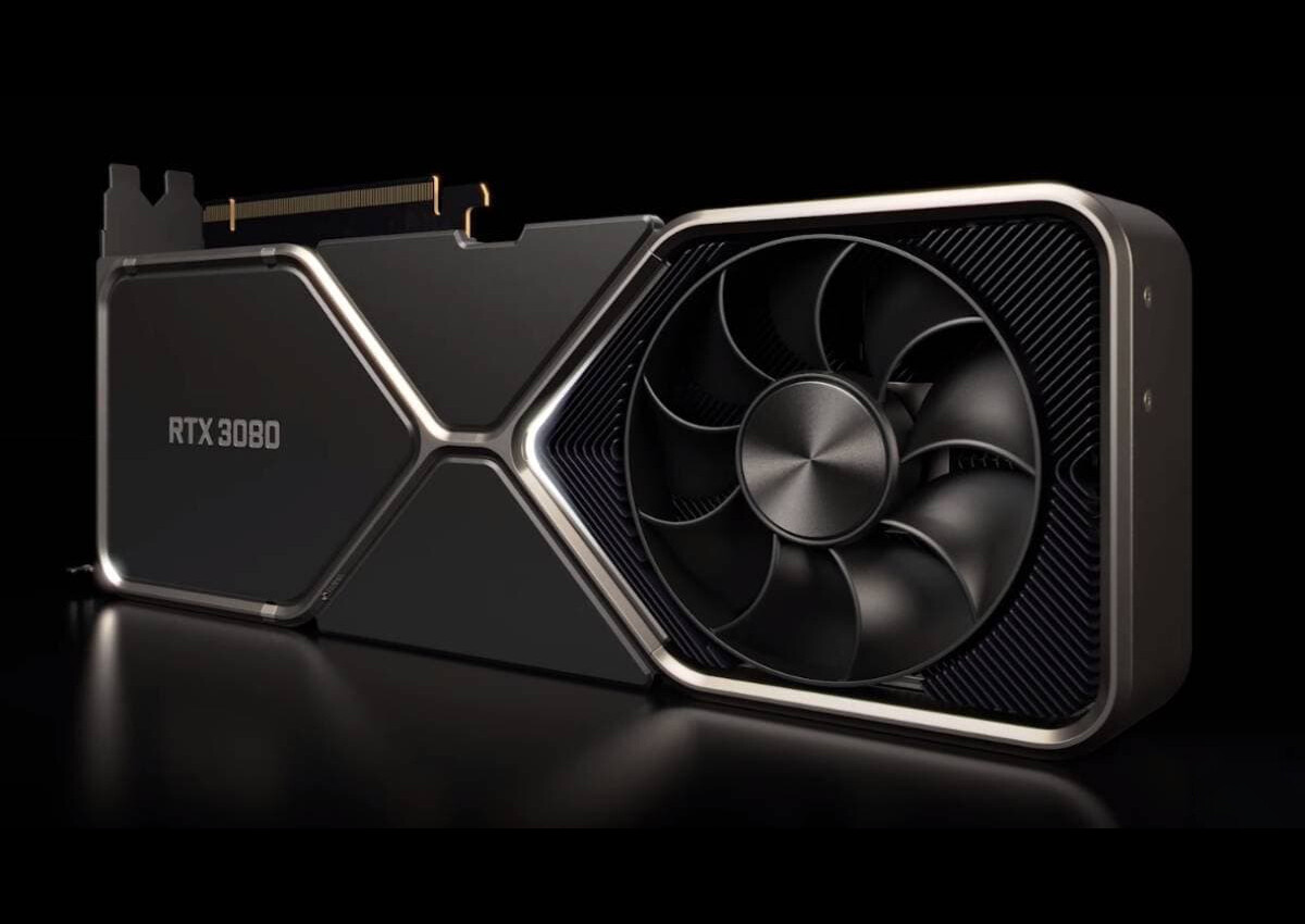
NVIDIA GeForce RTX 3080 12 GB Edition Rumored to Launch on January 11th
During the CES 2022 keynote, we have witnessed NVIDIA update its GeForce RTX 30 series family with GeForce RTX 3050 and RTX 3090 Ti. However, this is not an end to NVIDIA's updates to the Ampere generation, as we now hear industry sources from Wccftech suggest that we could see a GeForce RTX 3080 GPU with 12 GB of GDDR6X VRAM enabled, launched as a separate product. Compared to the regular RTX 3080 that carries only 10 GB of GDDR6X, the new 12 GB version is supposed to bring a slight bump up to the specification list. The GA102-220 GPU SKU found inside the 12 GB variant will feature 70 SMs with 8960 CUDA, 70 RT cores, and 280 TMUs.
This represents a minor improvement over the regular GA102-200 silicon inside the 8 GB model. However, the significant difference is the memory organization. With the new 12 GB model, we have a 384-bit memory bus allowing GDDR6X modules to achieve a bandwidth of 912 GB/s, all while running at 19 Gbps speeds. The overall TDP will also receive a bump to 350 Watts, compared to 320 Watts of the regular RTX 3080 model. For more information regarding final clock speeds and pricing, we have to wait for the alleged launch date - January 11th.
This represents a minor improvement over the regular GA102-200 silicon inside the 8 GB model. However, the significant difference is the memory organization. With the new 12 GB model, we have a 384-bit memory bus allowing GDDR6X modules to achieve a bandwidth of 912 GB/s, all while running at 19 Gbps speeds. The overall TDP will also receive a bump to 350 Watts, compared to 320 Watts of the regular RTX 3080 model. For more information regarding final clock speeds and pricing, we have to wait for the alleged launch date - January 11th.
AMD Zen 4 "Raphael" Processors Feature Improved Thermal Sensors and Power Management
AMD is slowly preparing the launch of the latest and greatest Ryzen processor family based on the Zen 4 CPU core design. Among various things that are getting an overhaul, the Raphael processor generation is now getting revamped temperature reading and better power management circuitry. According to an Igor's Lab report, AMD has prepared a few new improvements that will make temperature reading and power management easier for PC enthusiasts. Currently, the reported CPU temperature is called Tcontrol (Tctl), which is what the cooling solution sees. If Tctl is high, the fans spin up and cool the system. If Tctl is low, the fans slow down to reduce noise.
With Raphael, the CUR_TEMP (current temperature) output part of Tctl has been upgraded to reflect a much smoother curve, and avoid jittering with fans as they are not spiking so suddenly anymore. This is helping contribute to the noise output and has made it run at a consistent fan speed in the system. Another note about Raphael is a new power management technique. AMD has designed the AM5 platform to avoid sudden power spikes, to maintain maximum efficiency over time. It is a design decision made from the very start, and the CPU will try to constrain itself in the TDP range that it is configured for. For more details about the circuitry, please head over to the Igor's Lab article.
With Raphael, the CUR_TEMP (current temperature) output part of Tctl has been upgraded to reflect a much smoother curve, and avoid jittering with fans as they are not spiking so suddenly anymore. This is helping contribute to the noise output and has made it run at a consistent fan speed in the system. Another note about Raphael is a new power management technique. AMD has designed the AM5 platform to avoid sudden power spikes, to maintain maximum efficiency over time. It is a design decision made from the very start, and the CPU will try to constrain itself in the TDP range that it is configured for. For more details about the circuitry, please head over to the Igor's Lab article.

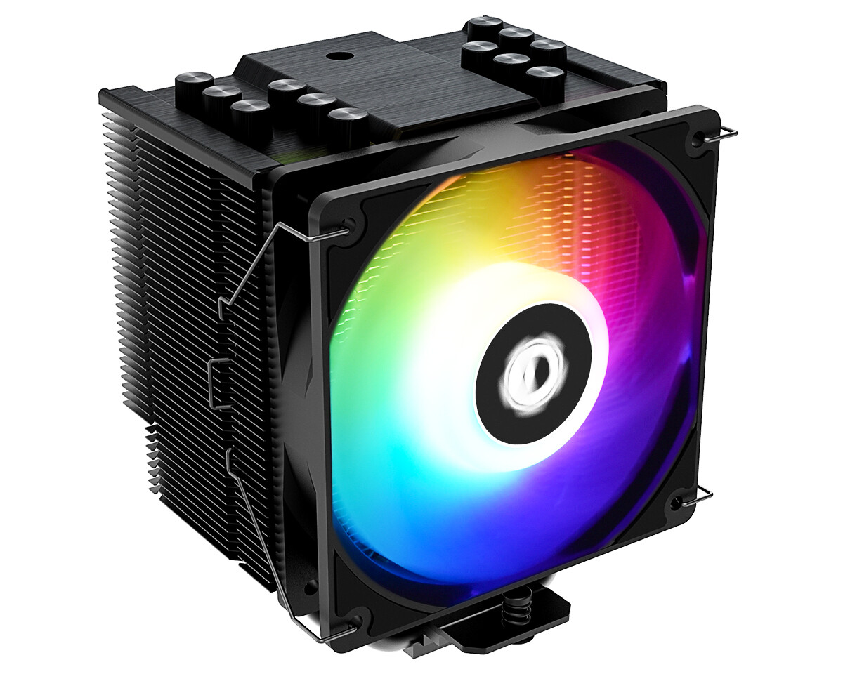
ID-COOLING Announces SE-226-XT CPU Air Coolers
ID-COOLING today announced SE-226-XT ARGB and SE-226-XT BLACK CPU air coolers. Both coolers include the same black heatsink with 6 heatpipes and copper base. 120 mm ARGB fan and Black fan are used on ARGB / BLACK version respectively. SE-226-XT Series is designed to cool those processors with a TDP up to 250 W. Both models are built with a solid heatsink which is specially design with 100% RAM compatibility. Black coating is applied for a stealthy looking.
For SE-226-XT ARGB, the included 120x120x25mm fan is built with 2Ball bearing and has 8pcs rubber dampeners on all corners of both sides, running at 800 to 2000rpm with PWM support while pushing 56.6CFM air at maximum speed, noise level measured 16.2 to 31.5dB (A). For SE-226-XT BLACK, the included standard 120x120x25mm fan has 8pcs rubber dampeners on all corners of both sides, running at 700 to 1800rpm with PWM support while pushing 76.16CFM air at maximum speed, noise level measured 15.2 to 35.2dB (A).

For SE-226-XT ARGB, the included 120x120x25mm fan is built with 2Ball bearing and has 8pcs rubber dampeners on all corners of both sides, running at 800 to 2000rpm with PWM support while pushing 56.6CFM air at maximum speed, noise level measured 16.2 to 31.5dB (A). For SE-226-XT BLACK, the included standard 120x120x25mm fan has 8pcs rubber dampeners on all corners of both sides, running at 700 to 1800rpm with PWM support while pushing 76.16CFM air at maximum speed, noise level measured 15.2 to 35.2dB (A).

Intel Core i7-12700 Geekbenched, Matches Ryzen 7 5800X
Intel's upcoming Core i7-12700 (non-K) processor matches AMD's Ryzen 7 5800X in the Geekbench 5 benchmark. The i7-12700 is a locked 65 W TDP processor with 8 "Golden Cove" P-cores, and 4 "Gracemont" E-cores. 4 fewer E-cores, lower clocks, and lack of features such as Thermal Velocity Boost, is what differentiates the 12th Gen Core i7 from 12th Gen Core i9.
The Core i7-12700 allegedly scored 1595 points single-thread, along with 10170 points in the multi-threaded test. This puts it within 5% of the Ryzen 7 5800X in the single-threaded test (averaged from the Geekbench database), and within 2% in the multi-threaded. One has to consider that the i7-12700 lacks an unlocked multiplier, but should Intel 600-series chipset motherboards come with the same power-limit unlocks as the 400-series and 500-series; more performance can be squeezed out.
The Core i7-12700 allegedly scored 1595 points single-thread, along with 10170 points in the multi-threaded test. This puts it within 5% of the Ryzen 7 5800X in the single-threaded test (averaged from the Geekbench database), and within 2% in the multi-threaded. One has to consider that the i7-12700 lacks an unlocked multiplier, but should Intel 600-series chipset motherboards come with the same power-limit unlocks as the 400-series and 500-series; more performance can be squeezed out.


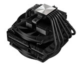
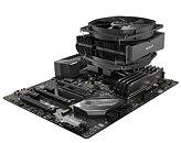
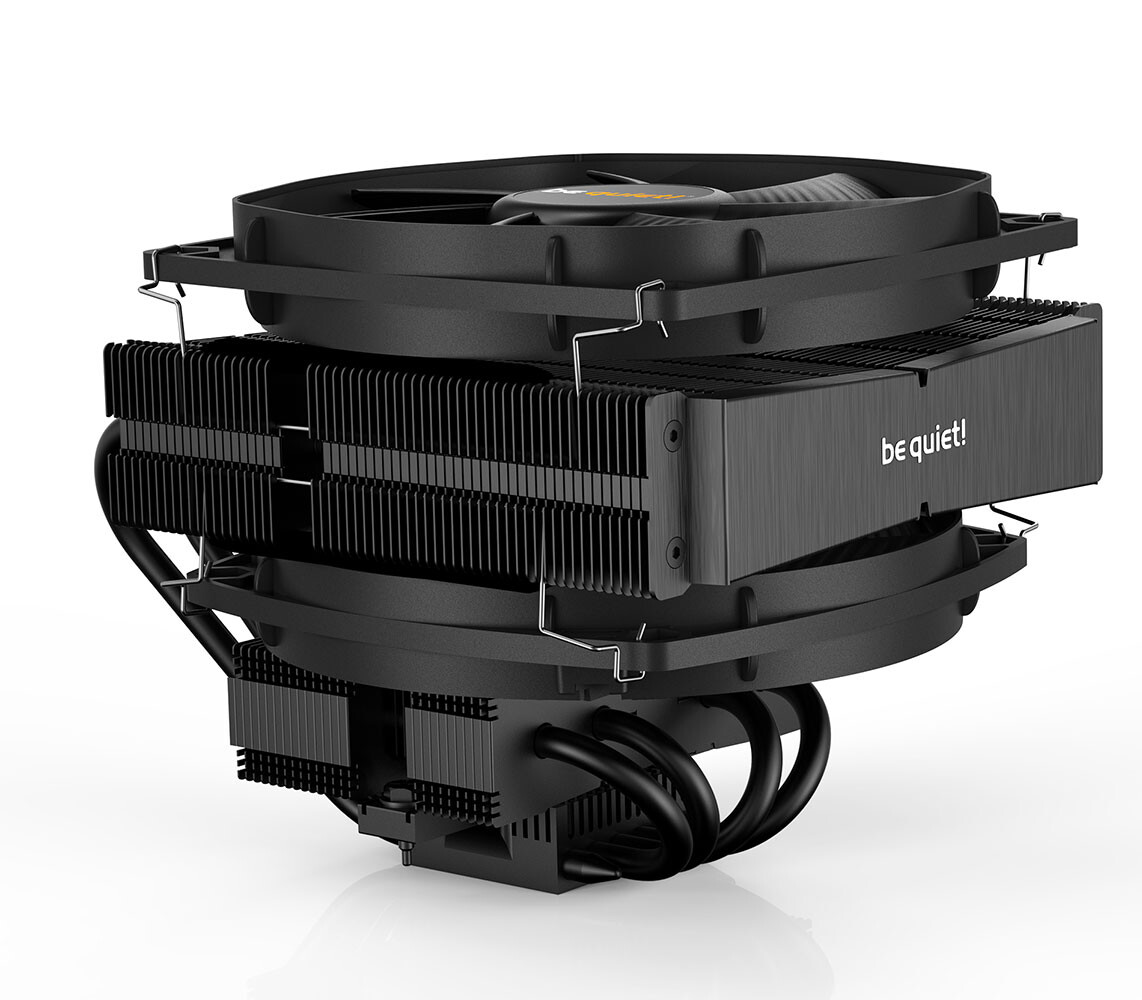
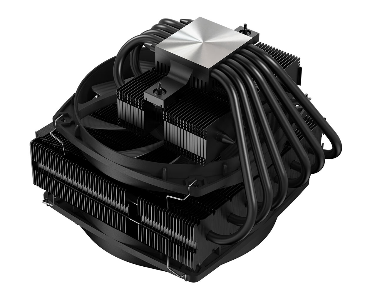
be quiet! Launches Dark Rock TF 2: High-end Cooling with Top-flow Design
be quiet!, the German manufacturer for premium PC components, is announcing Dark Rock TF 2. This high-end top-flow CPU cooler combines maximum cooling performance of up to 230 W TDP with virtually inaudible operation, thanks to its dual-heatsink design, six high-performance 6 mm heat pipes, and two Silent Wings 135 mm fans. Dark Rock TF 2 also looks the part with its brushed aluminium top cover and special black coating with ceramic particles, making it the ideal choice for all who strive for the highest yet quiet cooling performance in style.
For anyone looking for a true high-end cooler, Dark Rock TF 2 ticks all the right boxes. The dual-heatsink design with six high-performance copper heat pipes offers maximum performance even under extreme overclocking conditions and the top-flow design provides ideal cooling not only for the CPU but also for the surrounding motherboard components. Even so, Dark Rock TF 2 is virtually inaudible, thanks to a funnel-shaped Silent Wings 3 135 mm as the upper fan, and a Silent Wings 135 mm (without funnel-shaped entry) as the lower fan. Both fans are equipped with a durable fluid-dynamic bearing, smooth six-pole motors, and up to nine airflow-optimized fan blades, resulting in a low noise level of 27.1 dB(A) at 100% PWM speed. Anti-vibration rubber inserts on the heat sink fins further dampen unwanted operational sounds.

For anyone looking for a true high-end cooler, Dark Rock TF 2 ticks all the right boxes. The dual-heatsink design with six high-performance copper heat pipes offers maximum performance even under extreme overclocking conditions and the top-flow design provides ideal cooling not only for the CPU but also for the surrounding motherboard components. Even so, Dark Rock TF 2 is virtually inaudible, thanks to a funnel-shaped Silent Wings 3 135 mm as the upper fan, and a Silent Wings 135 mm (without funnel-shaped entry) as the lower fan. Both fans are equipped with a durable fluid-dynamic bearing, smooth six-pole motors, and up to nine airflow-optimized fan blades, resulting in a low noise level of 27.1 dB(A) at 100% PWM speed. Anti-vibration rubber inserts on the heat sink fins further dampen unwanted operational sounds.


GIGABYTE Releases the New Aorus WaterForce Series AIO Liquid Coolers
GIGABYTE TECHNOLOGY Co. Ltd, a leading manufacturer of motherboards, graphics cards, and hardware solutions today announced the new series of AIO liquid coolers - AORUS WATERFORCE SERIES, which come in 3 radiator sizes and fans corresponding to those different radiator dimensions. The new AIO coolers are available in 360 mm, 280 mm and 240 mm sizes to cater various needs. AORUS WATERFORCE SERIES support all modern and upcoming high performance multi-core CPU sockets. Besides the high compatibility with a multitude of builds, AORUS WATERFORCE SERIES inherit the advanced functions and designs from WATERFORCE X SERIES including the 330 degrees manually rotatable cap design that allows users to rotate the cap to adjust your preferred angle, the 7.8 mm Tube Diameter that improves the water flow by 37% and it's engineered with ceramic axis to optimize durability and heat-dissipation. The leading graphene Nano lubricant bearing with ultra-low friction and noise which reduces the carbon deposit while extending the life of the fan. According to the above, AORUS WATERFORCE SERIES provide enhanced heat-dissipation and durability. Even with 240 mm radiator, AORUS WATERFORCE delivers efficient heat-dissipation when running all-cores at 5.1 GHz on 8 cores pairing stress test with Intel Core i9-11900K processor.


Intel Core-1800 Alder Lake Engineering Sample Spotted with 16C/24T Configuration
Intel's upcoming Alder Lake generation of processors is going to be the first iteration of heterogeneous x86 architecture. That means that Intel will for the first time combine smaller, low-power cores, with some big high-performance cores to provide the boost to all the workloads. If a task doesn't need much power, as some background task, for example, the smaller cores are used. And if you need to render something or you want to fire up a game, big cores are used to provide the power needed for the tasks. Intel has decided to provide such an architecture on the advanced 10 nm SuperFin, which represents a major upgrade over the existing 14 nm process.
Today, we got some information from Igor's Lab, showing the leaked specification of the Intel Core-1800 processor engineering sample. While this may not represent the final name, we see that the leaked information shows that the processor is B0 stepping. That means that the CPU will see more changes when the final sample arrives. The CPU has 16 cores with 24 threads. Eight of those cores are big ones with hyperthreading, while the remaining 8 are smaller Atom cores. They are running at the base clock of 1800 MHz, while the boost speeds are 4.6 GHz with two cores, 4.4 GHz with four cores, and 4.2 GHz with 6 cores. When all cores are used, the boost speed is locked at 4.0 GHz. The CPU has a PL1 TDP of 125 Watts, while the PL2 configuration boosts the TDP to 228 Watts. The CPU was reportedly running at 1.3147 Volts during the test. You can check out the complete datasheet below.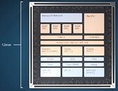

Today, we got some information from Igor's Lab, showing the leaked specification of the Intel Core-1800 processor engineering sample. While this may not represent the final name, we see that the leaked information shows that the processor is B0 stepping. That means that the CPU will see more changes when the final sample arrives. The CPU has 16 cores with 24 threads. Eight of those cores are big ones with hyperthreading, while the remaining 8 are smaller Atom cores. They are running at the base clock of 1800 MHz, while the boost speeds are 4.6 GHz with two cores, 4.4 GHz with four cores, and 4.2 GHz with 6 cores. When all cores are used, the boost speed is locked at 4.0 GHz. The CPU has a PL1 TDP of 125 Watts, while the PL2 configuration boosts the TDP to 228 Watts. The CPU was reportedly running at 1.3147 Volts during the test. You can check out the complete datasheet below.


AMD Launches Ryzen 5000G "Cezanne" APU Lineup for OEMs
AMD has today decided to launch the next generation of Accelerated Processing Units (APUs), now in form of the 5000G lineup codenamed Cezanne. The APUs are getting launched as OEM-exclusive products for now, which means that only manufacturers like Dell, HP, Lenovo, etc. can have access to them. AMD is set to announce these processors for wider masses, such as consumer DIYers, later this year. So you must be wondering what is new about the 5000G APUs. For starters, the new APUs feature AMD's improved Zen 3 core with a notable IPC boost over Zen 2 found in last generation 4000G APUs. When it comes to graphics, the new APUs feature anywhere from 6-8 GPU cores, based on the Vega architecture.
When it comes to the available models, AMD lists six SKUs, all differentiating in CPU/GPU core count, TDP, and frequency. There are three regular SKUs, with their power-efficient variants. The regular SKUs are AMD Ryzen 7 5700G, Ryzen 5 5600G, and Ryzen 3 5300G. They are normal SKUs that have a TDP of 65 Watts, meaning a higher base frequency needing a more adequate cooling solution. However, as there are regular SKUs, there are also power-efficient, TDP-constrained models present. Called the AMD Ryzen 7 5700GE, Ryzen 5 5600GE, and Ryzen 3 5300GE, these models bring the TDP down to 35 Watts and reduce base frequency by a couple of hundreds of MHz.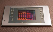
When it comes to the available models, AMD lists six SKUs, all differentiating in CPU/GPU core count, TDP, and frequency. There are three regular SKUs, with their power-efficient variants. The regular SKUs are AMD Ryzen 7 5700G, Ryzen 5 5600G, and Ryzen 3 5300G. They are normal SKUs that have a TDP of 65 Watts, meaning a higher base frequency needing a more adequate cooling solution. However, as there are regular SKUs, there are also power-efficient, TDP-constrained models present. Called the AMD Ryzen 7 5700GE, Ryzen 5 5600GE, and Ryzen 3 5300GE, these models bring the TDP down to 35 Watts and reduce base frequency by a couple of hundreds of MHz.
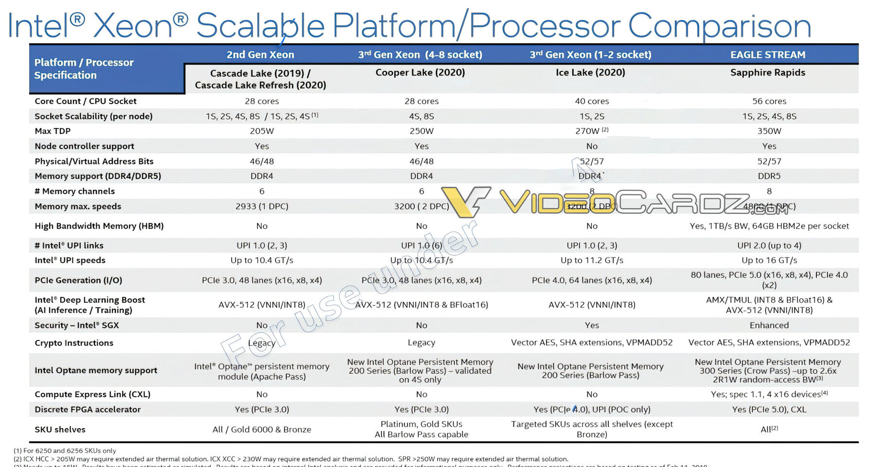
Intel's Upcoming Sapphire Rapids Server Processors to Feature up to 56 Cores with HBM Memory
Intel has just launched its Ice Lake-SP lineup of Xeon Scalable processors, featuring the new Sunny Cove CPU core design. Built on the 10 nm node, these processors represent Intel's first 10 nm shipping product designed for enterprise. However, there is another 10 nm product going to be released for enterprise users. Intel is already preparing the Sapphire Rapids generation of Xeon processors and today we get to see more details about it. Thanks to the anonymous tip that VideoCardz received, we have a bit more details like core count, memory configurations, and connectivity options. And Sapphire Rapids is shaping up to be a very competitive platform. Do note that the slide is a bit older, however, it contains useful information.
The lineup will top at 56 cores with 112 threads, where this processor will carry a TDP of 350 Watts, notably higher than its predecessors. Perhaps one of the most interesting notes from the slide is the department of memory. The new platform will make a debut of DDR5 standard and bring higher capacities with higher speeds. Along with the new protocol, the chiplet design of Sapphire Rapids will bring HBM2E memory to CPUs, with up to 64 GBs of it per socket/processor. The PCIe 5.0 standard will also be present with 80 lanes, accompanying four Intel UPI 2.0 links. Intel is also supposed to extend the x86_64 configuration here with AMX/TMUL extensions for better INT8 and BFloat16 processing.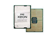
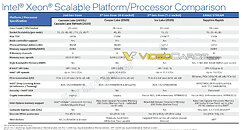
The lineup will top at 56 cores with 112 threads, where this processor will carry a TDP of 350 Watts, notably higher than its predecessors. Perhaps one of the most interesting notes from the slide is the department of memory. The new platform will make a debut of DDR5 standard and bring higher capacities with higher speeds. Along with the new protocol, the chiplet design of Sapphire Rapids will bring HBM2E memory to CPUs, with up to 64 GBs of it per socket/processor. The PCIe 5.0 standard will also be present with 80 lanes, accompanying four Intel UPI 2.0 links. Intel is also supposed to extend the x86_64 configuration here with AMX/TMUL extensions for better INT8 and BFloat16 processing.

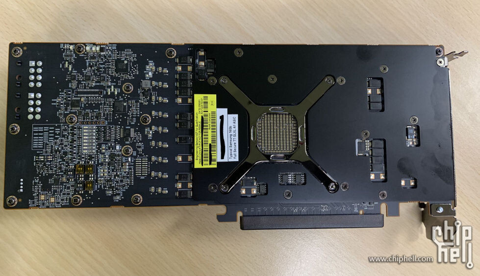
AMD Radeon Pro Workstation Card with Navi 21 GPU Pictured
When AMD introduced RDNA 2 architecture and higher-end Navi 21 GPU SKUs, it was only a matter of time before the company launches these GPUs inside professional-grade graphics cards. Today, thanks to the Chiphell forums, we have pictures and some specifications of AMD's upcoming Radeon Pro workstation graphics card. Pictured below is a new RDNA 2 based design that features AMD's Navi 21 GLXL GPU SKU. The new GLXL GPU SKU is supposed to be rather similar to the Navi 21 XL GPU found inside AMD's Radeon RX 6800 XT graphics card, judging by the number and arrangement of capacitors on the back of the card.
When it comes to memory, the upcoming Radeon Pro workstation card is featuring 16 GB of VRAM, likely a variant of GDDR6 found on gaming-oriented graphics cards from RDNA 2 generation. When it comes to cooler design, the Radeon Pro graphics card has a blower-type cooler helping tame the Navi 21 GLXL GPU. Given that blower-type coolers are suitable for situations with less airflow, the TDP of this card could be around or under 250 Watts. You can take a look at the card below, however, do note that it is an engineering sample and the final product can look a bit different.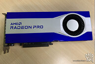
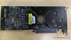
When it comes to memory, the upcoming Radeon Pro workstation card is featuring 16 GB of VRAM, likely a variant of GDDR6 found on gaming-oriented graphics cards from RDNA 2 generation. When it comes to cooler design, the Radeon Pro graphics card has a blower-type cooler helping tame the Navi 21 GLXL GPU. Given that blower-type coolers are suitable for situations with less airflow, the TDP of this card could be around or under 250 Watts. You can take a look at the card below, however, do note that it is an engineering sample and the final product can look a bit different.

Apr 22nd, 2025 03:38 EDT
change timezone
Latest GPU Drivers
New Forum Posts
- Yet another Case FAN topic and which Fans to choose (5)
- 5060 Ti 8GB DOA (116)
- What are you playing? (23415)
- am i alone to still using an asus p6t motherboard in the world ? (96)
- White Taichi 7900XTX (4)
- To distill or not distill what say ye? (34)
- Need thoughts on a quiet PC that's great for rendering, video editing and office work... (14)
- [Test Build] Fix for 576.02 Driver Install (44)
- Gainward Phoenix RTX 5070ti Temperatures (12)
- AAF Optimus Modded Driver For Windows 10 & Windows 11 - Only for Realtek HDAUDIO Chips (434)
Popular Reviews
- ASRock X870E Taichi Lite Review
- ASUS GeForce RTX 5060 Ti TUF OC 16 GB Review
- NVIDIA GeForce RTX 5060 Ti PCI-Express x8 Scaling
- Palit GeForce RTX 5060 Ti Infinity 3 16 GB Review
- MSI GeForce RTX 5060 Ti Gaming OC 16 GB Review
- Sapphire Radeon RX 9070 XT Pulse Review
- Upcoming Hardware Launches 2025 (Updated Apr 2025)
- Teevolution Terra Pro Review
- Sapphire Radeon RX 9070 XT Nitro+ Review - Beating NVIDIA
- ASUS GeForce RTX 5060 Ti Prime OC 16 GB Review
Controversial News Posts
- NVIDIA GeForce RTX 5060 Ti 16 GB SKU Likely Launching at $499, According to Supply Chain Leak (182)
- NVIDIA Sends MSRP Numbers to Partners: GeForce RTX 5060 Ti 8 GB at $379, RTX 5060 Ti 16 GB at $429 (127)
- NVIDIA Launches GeForce RTX 5060 Series, Beginning with RTX 5060 Ti This Week (115)
- Nintendo Confirms That Switch 2 Joy-Cons Will Not Utilize Hall Effect Stick Technology (105)
- Nintendo Switch 2 Launches June 5 at $449.99 with New Hardware and Games (99)
- Sony Increases the PS5 Pricing in EMEA and ANZ by Around 25 Percent (85)
- NVIDIA PhysX and Flow Made Fully Open-Source (77)
- Windows Notepad Gets Microsoft Copilot Integration (75)