Friday, April 9th 2021

Intel's Upcoming Sapphire Rapids Server Processors to Feature up to 56 Cores with HBM Memory
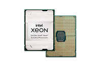
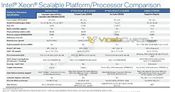
Intel has just launched its Ice Lake-SP lineup of Xeon Scalable processors, featuring the new Sunny Cove CPU core design. Built on the 10 nm node, these processors represent Intel's first 10 nm shipping product designed for enterprise. However, there is another 10 nm product going to be released for enterprise users. Intel is already preparing the Sapphire Rapids generation of Xeon processors and today we get to see more details about it. Thanks to the anonymous tip that VideoCardz received, we have a bit more details like core count, memory configurations, and connectivity options. And Sapphire Rapids is shaping up to be a very competitive platform. Do note that the slide is a bit older, however, it contains useful information.
The lineup will top at 56 cores with 112 threads, where this processor will carry a TDP of 350 Watts, notably higher than its predecessors. Perhaps one of the most interesting notes from the slide is the department of memory. The new platform will make a debut of DDR5 standard and bring higher capacities with higher speeds. Along with the new protocol, the chiplet design of Sapphire Rapids will bring HBM2E memory to CPUs, with up to 64 GBs of it per socket/processor. The PCIe 5.0 standard will also be present with 80 lanes, accompanying four Intel UPI 2.0 links. Intel is also supposed to extend the x86_64 configuration here with AMX/TMUL extensions for better INT8 and BFloat16 processing.
Source:
VideoCardz
The lineup will top at 56 cores with 112 threads, where this processor will carry a TDP of 350 Watts, notably higher than its predecessors. Perhaps one of the most interesting notes from the slide is the department of memory. The new platform will make a debut of DDR5 standard and bring higher capacities with higher speeds. Along with the new protocol, the chiplet design of Sapphire Rapids will bring HBM2E memory to CPUs, with up to 64 GBs of it per socket/processor. The PCIe 5.0 standard will also be present with 80 lanes, accompanying four Intel UPI 2.0 links. Intel is also supposed to extend the x86_64 configuration here with AMX/TMUL extensions for better INT8 and BFloat16 processing.


29 Comments on Intel's Upcoming Sapphire Rapids Server Processors to Feature up to 56 Cores with HBM Memory
Im hoping consumer platforms will get most of it trickled down. The idea of HEDT for Intel died the moment Threadripper first gen came out, pretty much.
Who knows.
10nm still looks broken to me, although there's no mention of clockspeeds at that power draw, so maybe they've ironed out enough kinks to be competitive.
These are datacenter parts. Performance per Watt is king there and AMD already has Zen3 Epyc with 64C/128 and 2P support at 225W. Embarassingly cheap compared to Xeon Platinums, too.
You can do it, you can reach 64 cores, someday, preferrably at less power consumption too.
I just spotted that Anandtech have reviewed 3rd Gen Xeon and whilst it's not a turd, yeah it's not looking good either. To say it's better than the dumpster fire of previous-gen Xeons is a veiled insult. Maybe they're approaching AMD's older Rome (Zen2) Epyc lineup in performance and efficiency, so they're now only 2 years behind.
It looks like 10nm is still not good, but it's come far enough that it's now worth using over Skylake 14nm from 2017.
@HalfAHertz
This is Intel's first stab at glue in a long time and they're not very good at it. Reminds me of the power/efficiency scaling of Core2Quad :D
I'm guessing that these are going to be intended for supercomputers, as a competitor to the A64Fx, and not as a typical datacenter CPU.
The problem with those processors was that they only came from one source - Intel-built servers. The highest model having 56 cores required liquid cooling since it had a TDP of 400W:
HBM2 is maybe slightly more latency to DDR4 / DDR5 and higher bandwidth. That makes it complicated to reason about. There will be many cases where HBM2 slows down code (any latency-critical code), while speeding up other cases (speeds up bandwidth-critical code). As far as I'm aware, no one has ever figured out a way to predict whether code is latency bound or bandwidth bound ahead of time.
-------
One of the Xeon Phi models had HMC (a competitor to HBM) + DDR4. And look how well that was figured out. Its hard as hell to optimize programs on those kinds of split-memory systems. There were all sorts of issues figuring out whether or not something should be in the HMC or on the DDR4.
software.intel.com/content/www/us/en/develop/articles/intel-xeon-phi-processor-7200-family-memory-management-optimizations.html
Its not easy. Just give Xeon Phi 7200 documents a look, and then imagine trying to write code against that.
The thing is, if whatever it is that you wrote is highly multithreaded and data independent latency typically doesn't matter.
Lol. Single-threaded, highly-dependent data being passed around, turning into XML into protobufs, back into XML, and then converted into JSON just to pass 50-bytes of text around. Yeaaaahhhhhhhh. Better companies may have good programmers who write more intelligent code. But seriously: most code out there (even "enterprise" code) is absolute unoptimized single-threaded crap.
every console built and optimized program built is coded and tuned for the performance of the hardware being used, an additional level of cache that is that close and finely tuned will boost performance compared to system memory and can be further tuned when the specifics are known.
this is why the consoles can have actual higher performance than X86 running generic code to fit all configuration.
even if it nets a 10 percent performance boost Intel needs it to stay competitive.
- Second-gen 10nm in Sunny Cove clocked poorly at the top end, which placed 4.0GHz generally out of reach.
- Third-gen 10SF in Willow Cove only improved that frequency scaling at the top end, relevant only really for consumer parts.
- 10ESF for Willow Cove might improve by the same small margin efficiency-wise as 10SF, just increasing the clock envelope further.
The process hasn't changed much in the 2.0-3.5GHz range, which is where Xeons reside. Neither has the arch changed much. So add more cores (and more chiplets) like Intel is doing here, and power's just gonna go up - no surprises there.I was foolishly thinking this might be a sign that 10nm desktop parts are on the way in 2021 but actually, low-clock server parts can be viable whilst the process node is still wholly useless for consumer products at 4GHz+
I actually wish Intel would go back to making fanless CPUs - the sub 5W Core-M range was great for ultraportables and they ran at 0.8-2.0GHz which would be plenty for a general-purpose laptop. My experience with Ice Lake 10nm laptops was that they cooked themselves when boosting but otherwise ran very efficiently. What if Intel made a 4C/8T CPU with a 5W envelope and max clockspeed of, say, 1.6GHz? I'd buy that.
People are touting Hbm memory near CPU to help ai and ml applications specifically.
I would imagine the plan is to have tiered memory personally, not to use it as a l4 cache but rather a special pool to use as required depending on the application.
Given Intel always has a wide array of SKU's it's relatively easy to imagine that Hbm won't be on every SKU since some applications might not require it.
And whatever gets written in that way is probably not something performance critical anyway.
In fact, most DDR4 / HBM / GDDR6x "latency improvements" aren't actually improving latency at all. They're just hiding latency behind more-and-more parallel requests. See DDR4 bank-groups. They're up to 32 parallel bank groups (and therefore 32-parallel PRE-RAS-CAS sequences) per chip in DDR4 IIRC, and that will only go up.
Whenever we start seeing eDRAM / DRAM as a caching layer (ex: XBox 360, Xeon Phi 7200), we suddenly get an influx of frustrated programmers who have to deal with the reality of the architecture. You're simply not going to get much better than the ~50ns or so of latency on DRAM. Too many steps need to be done per request at the fundamental physics layer.
SRAM (typical L3 / L2 / L1 caches) just doesn't have to deal with any of those steps at all. So adding those caches and/or making them bigger is simple and obvious.
Also... the Data Streaming Accelerator is an interesting addition. Its spec says it supports Optane. There is also an operation for flushing processor cache.
I wonder if the DSA is being used to maintain the processor cache coherency with accelerator memory when CXL bias ownership is flipped.