Apr 18th, 2025 15:03 EDT
change timezone
Latest GPU Drivers
New Forum Posts
- What are you playing? (23396)
- TPU's Nostalgic Hardware Club (20256)
- Can Intel recover in DYI market anytime soon? (7)
- Spoofer Modified SMBIOS/BIOS – Need Help Restoring Original Motherboard Info (TUF GAMING B550-PLUS WiFi II) (2)
- Tried installing 576.02 - installer window disappears (20)
- GPU Pricing and Performance (14)
- Place your bets, what node will rtx 6000/RDNA 5(UDNA 1?) use (6)
- RX 9000 series GPU Owners Club (392)
- GPU Database (300)
- Drives fail to work with Rufus Windows TO GO (2)
Popular Reviews
- ASUS GeForce RTX 5060 Ti TUF OC 16 GB Review
- NVIDIA GeForce RTX 5060 Ti PCI-Express x8 Scaling
- Palit GeForce RTX 5060 Ti Infinity 3 16 GB Review
- G.SKILL Trident Z5 NEO RGB DDR5-6000 32 GB CL26 Review - AMD EXPO
- ASUS GeForce RTX 5060 Ti Prime OC 16 GB Review
- MSI GeForce RTX 5060 Ti Gaming OC 16 GB Review
- Zotac GeForce RTX 5060 Ti AMP 16 GB Review
- Teevolution Terra Pro Review
- MSI GeForce RTX 5060 Ti Gaming Trio OC 16 GB Review
- ASUS GeForce RTX 5080 TUF OC Review
Controversial News Posts
- NVIDIA GeForce RTX 5060 Ti 16 GB SKU Likely Launching at $499, According to Supply Chain Leak (182)
- NVIDIA Sends MSRP Numbers to Partners: GeForce RTX 5060 Ti 8 GB at $379, RTX 5060 Ti 16 GB at $429 (127)
- Nintendo Confirms That Switch 2 Joy-Cons Will Not Utilize Hall Effect Stick Technology (105)
- Over 200,000 Sold Radeon RX 9070 and RX 9070 XT GPUs? AMD Says No Number was Given (100)
- Nintendo Switch 2 Launches June 5 at $449.99 with New Hardware and Games (99)
- NVIDIA Launches GeForce RTX 5060 Series, Beginning with RTX 5060 Ti This Week (98)
- Sony Increases the PS5 Pricing in EMEA and ANZ by Around 25 Percent (85)
- NVIDIA PhysX and Flow Made Fully Open-Source (77)
News Posts matching #HBM
Return to Keyword Browsing
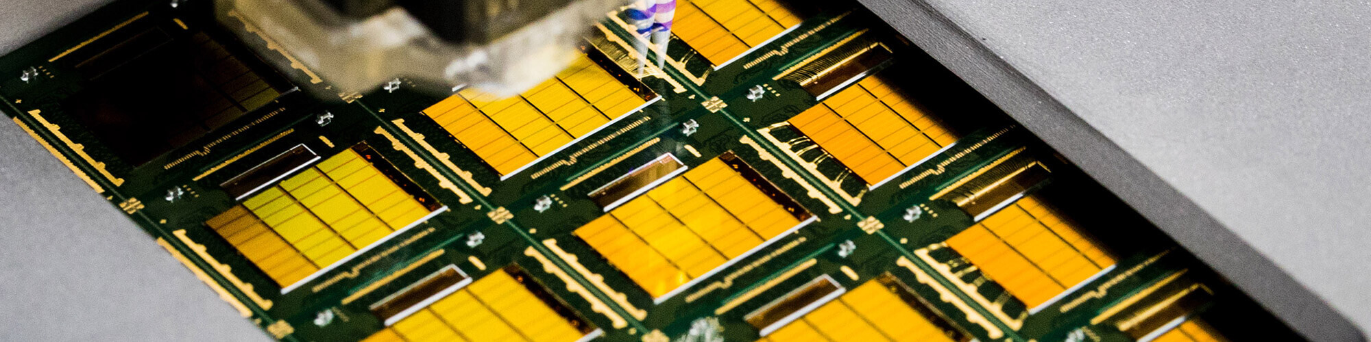
Micron Announces Business Unit Reorganization to Capitalize on AI Growth Across All Market Segments
Micron Technology, Inc. (Nasdaq: MU), a leader in innovative memory and storage solutions, today announced a market segment-based reorganization of its business units to capitalize on the transformative growth driven by AI, from data centers to edge devices.
Micron has maintained multiple generations of industry leadership in DRAM and NAND technology and has the strongest competitive positioning in its history. Micron's industry-leading product portfolio, combined with world-class manufacturing execution enables the development of differentiated solutions for its customers across end markets. As high-performance memory and storage become increasingly vital to drive the growth of AI, this Business Unit reorganization will allow Micron to stay at the forefront of innovation in each market segment through deeper customer engagement to address the dynamic needs of the industry.
Micron has maintained multiple generations of industry leadership in DRAM and NAND technology and has the strongest competitive positioning in its history. Micron's industry-leading product portfolio, combined with world-class manufacturing execution enables the development of differentiated solutions for its customers across end markets. As high-performance memory and storage become increasingly vital to drive the growth of AI, this Business Unit reorganization will allow Micron to stay at the forefront of innovation in each market segment through deeper customer engagement to address the dynamic needs of the industry.

US Bans Export of NVIDIA H20 Accelerators to China, a Potential $5.5 Billion Loss for NVIDIA
President Trump's administration has announced that NVIDIA's H20 AI chip will require a special export license for any shipment to China, Hong Kong, or Macau for the indefinite future. The Commerce Department delivered the news to NVIDIA on April 14, 2025, citing worries that the H20 could be redirected into Chinese supercomputers with potential military applications. NVIDIA designed the H20 specifically to comply with earlier US curbs by scaling back performance from its flagship H100 model. The H20 features 96 GB of HBM3 memory running at up to 4.0 TB/s, delivers roughly 296 TeraFLOPS of mixed‑precision compute power, and offers a performance density of about 2.9 TeraFLOPS per die. Its single‑precision (FP32) throughput is around 74 TeraFLOPS, with FP16 performance reaching approximately 148 TeraFLOPS. In a regulatory filing on April 15, NVIDIA warned that it will record about $5.5 billion in writedowns this quarter related to H20 inventory and purchase commitments now blocked by the license requirement.
Shares of NVIDIA fell roughly 6 percent in after‑hours trading on April 15, triggering a wider sell‑off in semiconductor stocks from the US to Japan. South Korea's Samsung and SK Hynix each slid about 3 percent, while AMD also dropped on concerns about broader chip‑export curbs. Analysts at Bloomberg Intelligence project that, if the restrictions persist, NVIDIA's China‑related data center revenue could shrink to low‑ or mid‑single digits as a percentage of total sales, down from roughly 13 percent in fiscal 2024. Chinese AI players such as Huawei stand to gain as customers seek alternative inference accelerators. Commerce Secretary Howard Lutnick has pledged to maintain a tough stance on chip exports to China even as NVIDIA commits up to $500 billion in US AI infrastructure investments over the next four years. Everyone is now watching closely to see whether any H20 export licenses are approved and how long the ban might remain in place.
Shares of NVIDIA fell roughly 6 percent in after‑hours trading on April 15, triggering a wider sell‑off in semiconductor stocks from the US to Japan. South Korea's Samsung and SK Hynix each slid about 3 percent, while AMD also dropped on concerns about broader chip‑export curbs. Analysts at Bloomberg Intelligence project that, if the restrictions persist, NVIDIA's China‑related data center revenue could shrink to low‑ or mid‑single digits as a percentage of total sales, down from roughly 13 percent in fiscal 2024. Chinese AI players such as Huawei stand to gain as customers seek alternative inference accelerators. Commerce Secretary Howard Lutnick has pledged to maintain a tough stance on chip exports to China even as NVIDIA commits up to $500 billion in US AI infrastructure investments over the next four years. Everyone is now watching closely to see whether any H20 export licenses are approved and how long the ban might remain in place.
Huawei CloudMatrix 384 System Outperforms NVIDIA GB200 NVL72
Huawei announced its CloudMatrix 384 system super node, which the company touts as its own domestic alternative to NVIDIA's GB200 NVL72 system, with more overall system performance but worse per-chip performance and higher power consumption. While NVIDIA's GB200 NVL72 uses 36 Grace CPUs paired with 72 "Blackwell" GB200 GPUs, the Huawei CloudMatrix 384 system employs 384 Huawei Ascend 910C accelerators to beat NVIDIA's GB200 NVL72 system. It takes roughly five times more Ascend 910C accelerators to deliver nearly twice the GB200 NVL system performance, which is not good on per-accelerator bias, but excellent on per-system level of deployment. SemiAnalysis argues that Huawei is a generation behind in chip performance but ahead of NVIDIA in scale-up system design and deployment.
When you look at individual chips, NVIDIA's GB200 NVL72 clearly outshines Huawei's Ascend 910C, delivering over three times the BF16 performance (2,500 TeraFLOPS vs. 780 TeraFLOPS), more on‑chip memory (192 GB vs. 128 GB), and faster bandwidth (8 TB/s vs. 3.2 TB/s). In other words, NVIDIA has the raw power and efficiency advantage at the chip level. But flip the switch to the system level, and Huawei's CloudMatrix CM384 takes the lead. It cranks out 1.7× the overall PetaFLOPS, packs in 3.6× more total HBM capacity, and supports over five times the number of GPUs and the associated bandwidth of NVIDIA's NVL72 cluster. However, that scalability does come with a trade‑off, as Huawei's setup draws nearly four times more total power. A single GB200 NVL72 draws 145 kW of power, while a single Huawei CloudMatrix 384 draws ~560 kW. So, NVIDIA is your go-to if you need peak efficiency in a single GPU. If you're building a massive AI supercluster where total throughput and interconnect speed matter most, Huawei's solution actually makes a lot of sense. Thanks to its all-to-all topology, Huawei has delivered an AI training and inference system worth purchasing. When SMIC, the maker of Huawei's chips, gets to a more advanced manufacturing node, the efficiency of these systems will also increase.

When you look at individual chips, NVIDIA's GB200 NVL72 clearly outshines Huawei's Ascend 910C, delivering over three times the BF16 performance (2,500 TeraFLOPS vs. 780 TeraFLOPS), more on‑chip memory (192 GB vs. 128 GB), and faster bandwidth (8 TB/s vs. 3.2 TB/s). In other words, NVIDIA has the raw power and efficiency advantage at the chip level. But flip the switch to the system level, and Huawei's CloudMatrix CM384 takes the lead. It cranks out 1.7× the overall PetaFLOPS, packs in 3.6× more total HBM capacity, and supports over five times the number of GPUs and the associated bandwidth of NVIDIA's NVL72 cluster. However, that scalability does come with a trade‑off, as Huawei's setup draws nearly four times more total power. A single GB200 NVL72 draws 145 kW of power, while a single Huawei CloudMatrix 384 draws ~560 kW. So, NVIDIA is your go-to if you need peak efficiency in a single GPU. If you're building a massive AI supercluster where total throughput and interconnect speed matter most, Huawei's solution actually makes a lot of sense. Thanks to its all-to-all topology, Huawei has delivered an AI training and inference system worth purchasing. When SMIC, the maker of Huawei's chips, gets to a more advanced manufacturing node, the efficiency of these systems will also increase.


Safe Superintelligence Inc. Uses Google TPUs Instead of Regular GPUs for Next-Generation Models
It seems like Google aims to grab a bit of the market share from NVIDIA and AMD by offering startups large compute deals and allowing them to train their massive AI models on the Google Cloud Platform (GCP). One such case is the OpenAI co-founder Ilya Sutskever's Safe Superintelligence Inc. (SSI) startup. According to a GCP post, SSI is "partnering with Google Cloud to use TPUs to accelerate its research and development efforts toward building a safe, superintelligent AI." Google's latest TPU v7p, codenamed Ironwood, was released yesterday. Carrying 4,614 TeraFLOPS of FP8 precision and 192 GB of HBM memory, these TPUs are interconnected using Google's custom ICI infrastructure and are scaled to configurations in pods of 9,216 chips, where Ironwood delivers 42.5 ExaFLOPS of total computing power.
For AI training, this massive power will allow AI models to quickly go over training, accelerating research iterations and ultimately accelerating model development. For SSI, the end goal is a simple mission: achieving ASI with safety at the front. "We approach safety and capabilities in tandem, as technical problems to be solved through revolutionary engineering and scientific breakthroughs. We plan to advance capabilities as fast as possible while making sure our safety always remains ahead," notes the SSI website, adding that "Our singular focus means no distraction by management overhead or product cycles, and our business model means safety, security, and progress are all insulated from short-term commercial pressures."
For AI training, this massive power will allow AI models to quickly go over training, accelerating research iterations and ultimately accelerating model development. For SSI, the end goal is a simple mission: achieving ASI with safety at the front. "We approach safety and capabilities in tandem, as technical problems to be solved through revolutionary engineering and scientific breakthroughs. We plan to advance capabilities as fast as possible while making sure our safety always remains ahead," notes the SSI website, adding that "Our singular focus means no distraction by management overhead or product cycles, and our business model means safety, security, and progress are all insulated from short-term commercial pressures."

Google Unveils Seventh-Generation AI Processor: Ironwood
Google has rolled out its seventh-generation AI chip, Ironwood, which aims to boost AI application performance. This processor focuses on "inference" computing—the quick calculations needed for chatbot answers and other AI outputs. Ironwood stands as one of the few real options to NVIDIA's leading AI processors coming from Google's ten-year multi-billion-dollar push to develop it. These tensor processing units (TPUs) are exclusively available through Google's cloud service or to its internal engineers.
According to Google Vice President Amin Vahdat, Ironwood combines functions from previously separate designs while increasing memory capacity. The chip can operate in groups of up to 9,216 processors and delivers twice the performance-per-energy ratio compared to last year's Trillium chip. When configured in pods of 9,216 chips, Ironwood delivers 42.5 Exaflops of computing power. This is more than 24 times the computational capacity of El Capitan, currently the world's largest supercomputer, which provides only 1.7 Exaflops per pod.

According to Google Vice President Amin Vahdat, Ironwood combines functions from previously separate designs while increasing memory capacity. The chip can operate in groups of up to 9,216 processors and delivers twice the performance-per-energy ratio compared to last year's Trillium chip. When configured in pods of 9,216 chips, Ironwood delivers 42.5 Exaflops of computing power. This is more than 24 times the computational capacity of El Capitan, currently the world's largest supercomputer, which provides only 1.7 Exaflops per pod.


Altera Starts Production Shipments of Agilex 7 FPGA M-Series
Altera Corporation, a leader in FPGA innovations, today announced production shipments of its Agilex 7 FPGA M-Series, the industry's first high-end, high-density FPGA to feature integrated high bandwidth memory and support for DDR5 and LPDDR5 memory technologies. Offering over 3.8 million logic elements, Agilex 7 FPGA M-Series is optimized for applications that demand the highest performance and highest memory bandwidth, including AI, data centers, next-generation firewalls, 5G communications infrastructure and 8K broadcast equipment.
As data traffic continues to increase exponentially due to the growth of AI, cloud computing and video streaming services, the demand for higher memory bandwidth, increased capacity, and improved power efficiency has never been greater. Agilex 7 FPGA M-Series addresses these challenges by offering users high logic densities, a high-performance fabric and a memory interface that accelerates data throughput speeds while reducing memory bottlenecks and latency.
As data traffic continues to increase exponentially due to the growth of AI, cloud computing and video streaming services, the demand for higher memory bandwidth, increased capacity, and improved power efficiency has never been greater. Agilex 7 FPGA M-Series addresses these challenges by offering users high logic densities, a high-performance fabric and a memory interface that accelerates data throughput speeds while reducing memory bottlenecks and latency.

Micron Announces Memory Price Increases for 2025-2026 Amid Supply Constraints
In a letter to customers, Micron has announced upcoming memory price increases extending through 2025 and 2026, citing persistent supply constraints coupled with accelerating demand across its product portfolio. The manufacturer points to significant demand growth in DRAM, NAND flash, and high-bandwidth memory (HBM) segments as key drivers behind the pricing strategy. The memory market is rebounding from a prolonged oversupply cycle that previously depressed revenues industry-wide. Strategic production capacity reductions implemented by major suppliers have contributed to price stabilization and subsequent increases over the past twelve months. This pricing trajectory is expected to continue as data center operators, AI deployments, and consumer electronics manufacturers compete for limited memory allocation.
In communications to channel partners, Micron emphasized AI and HPC requirements as critical factors necessitating the price adjustments. The company has requested detailed forecast submissions from partners to optimize production planning and supply chain stability during the constrained market period. With its pricing announcement, Micron disclosed a $7 billion investment in a Singapore-based HBM assembly facility. The plant will begin operations in 2026 and will focus on HBM3E, HBM4, and HBM4E production—advanced memory technologies essential for next-generation AI accelerators and high-performance computing applications from NVIDIA, AMD, Intel, and other companies. The price increases could have cascading effects across the AI and GPU sector, potentially raising costs for products ranging from consumer gaming systems to enterprise data infrastructure. We are monitoring how these adjustments will impact hardware refresh cycles and technology adoption rates as manufacturers pass incremental costs to end customers.
In communications to channel partners, Micron emphasized AI and HPC requirements as critical factors necessitating the price adjustments. The company has requested detailed forecast submissions from partners to optimize production planning and supply chain stability during the constrained market period. With its pricing announcement, Micron disclosed a $7 billion investment in a Singapore-based HBM assembly facility. The plant will begin operations in 2026 and will focus on HBM3E, HBM4, and HBM4E production—advanced memory technologies essential for next-generation AI accelerators and high-performance computing applications from NVIDIA, AMD, Intel, and other companies. The price increases could have cascading effects across the AI and GPU sector, potentially raising costs for products ranging from consumer gaming systems to enterprise data infrastructure. We are monitoring how these adjustments will impact hardware refresh cycles and technology adoption rates as manufacturers pass incremental costs to end customers.

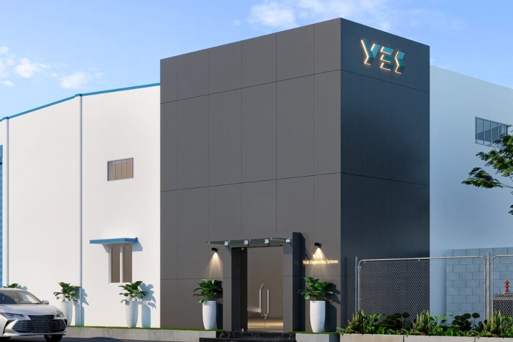
YES Pioneers Semiconductor Equipment Production in India
Yield Engineering Systems, Inc. (YES), a global leader in materials and interface engineering equipment solutions, proudly announces the shipment of the first commercial VeroTherm Formic Acid Reflow tool to a leading global semiconductor manufacturer from its Sulur, Coimbatore, manufacturing facility. This landmark achievement signifies a pivotal moment for YES and the burgeoning semiconductor ecosystem in India, as it represents the first equipment produced in India for advanced semiconductor applications like High Bandwidth Memory (HBM), which is critical for AI and High-Performance Computing (HPC) applications worldwide.
YES commenced operations in September 2024 at this state-of-the-art manufacturing facility in Sulur, Coimbatore, India, located at 96/3 Vadakku Sambala Thottam, Trichy Road, Kannampalayam, Sulur Taluk. This facility is integral to YES's strategic expansion plan, aimed at serving its global customers' operations in India and the world with greater efficiency.
YES commenced operations in September 2024 at this state-of-the-art manufacturing facility in Sulur, Coimbatore, India, located at 96/3 Vadakku Sambala Thottam, Trichy Road, Kannampalayam, Sulur Taluk. This facility is integral to YES's strategic expansion plan, aimed at serving its global customers' operations in India and the world with greater efficiency.
Sarcina Technology Launches AI Chiplet Platform Enabling Systems Up to 100x100 mm in a Single Package
Sarcina Technology, a global semiconductor packaging specialist, is excited to announce the launch of its innovative AI platform to enable advanced AI packaging solutions that can be tailored to meet specific customer requirements. Leveraging ASE's FOCoS-CL (Fan-Out Chip-on-Substrate-Chip Last) assembly technology, this platform includes an interposer which supports chiplets using UCIe-A for die-to-die interconnects, allowing for the delivery of cost-effective, customizable, cutting-edge solutions.
Sarcina Technology is on a mission to push the boundaries of AI computing system development by providing a unique platform that enables efficient, scalable, configurable and cost-effective semiconductor packaging solutions for AI applications. As AI workloads continue to evolve, there is a need for increasingly sophisticated packaging solutions capable of supporting higher computational demands. Sarcina's novel interposer packaging technology integrates leading memory solutions with high-efficiency interconnects. Whether prioritizing cost, performance or power-efficiency, Sarcina's new AI platform can deliver.
Sarcina Technology is on a mission to push the boundaries of AI computing system development by providing a unique platform that enables efficient, scalable, configurable and cost-effective semiconductor packaging solutions for AI applications. As AI workloads continue to evolve, there is a need for increasingly sophisticated packaging solutions capable of supporting higher computational demands. Sarcina's novel interposer packaging technology integrates leading memory solutions with high-efficiency interconnects. Whether prioritizing cost, performance or power-efficiency, Sarcina's new AI platform can deliver.

Downstream Inventory Reduction Eases DRAM Price Decline in 2Q25
TrendForce's latest findings reveal that U.S. tariff hikes prompted most downstream brands to frontload shipments to 1Q25, accelerating inventory reduction across the memory supply chain. Looking ahead to the second quarter, conventional DRAM prices are expected to decline by just 0-5% QoQ, while average DRAM pricing including HBM is forecast to rise by 3-8%, driven by increasing shipments of HBM3e 12hi.
PC and server DRAM prices to hold steady
In response to potential U.S. tariff hikes, major PC OEMs are requesting ODMs to increase production, accelerating DRAM depletion in their inventories. OEMs with lower inventory levels may raise procurement from suppliers in Q2 to ensure stable DRAM supply for the second half of 2025.

SK hynix Showcases Industry-Leading Memory Technology at GTC 2025
SK hynix Inc. announced today that it will participate in the GTC 2025, a global AI conference taking place March 17-21 in San Jose, California, with a booth titled "Memory, Powering AI and Tomorrow". The company will present HBM and other memory products for AI data centers and on-device and memory solutions for automotive business essential for AI era.
Among the industry-leading AI memory technology to be displayed at the show are 12-high HBM3E and SOCAMM (Small Outline Compression Attached Memory Module), a new memory standard for AI servers.

Among the industry-leading AI memory technology to be displayed at the show are 12-high HBM3E and SOCAMM (Small Outline Compression Attached Memory Module), a new memory standard for AI servers.


Huawei Obtained Two Million Ascend 910B Dies from TSMC via Shell Companies to Circumvent US Sanctions
According to a recent Center for Strategic and International Studies report, Huawei got its hand on approximately two million Ascend 910B logic dies through shell companies that misled TSMC. This acquisition violates US export controls designed to restrict China's access to advanced semiconductor technology. The report details how Huawei leveraged intermediaries to procure chiplets for its AI accelerators before TSMC discovered the deception and halted shipments. These components are critical for Huawei's AI hardware roadmap, which progressed from the original Ascend 910 (manufactured by TSMC on N7+ until 2020) to the domestically produced Ascend 910B and 910C chips fabricated at SMIC using first and second-generation 7 nm-class technologies, respectively. Huawei reportedly wanted TSMC-made dies because of manufacturing challenges in domestic chip production. The Ascend 910B and 910C reportedly suffer from poor yields, with approximately 25% of units failing during the advanced packaging process that combines compute dies with HBM memory.
Despite these challenges, the performance gap with market-leading solutions still remains but has narrowed considerably, with the Ascend 910C reportedly delivering 60% of NVIDIA H100's performance. Huawei has executed a strategic stockpiling initiative, particularly for high-bandwidth memory components. The company likely acquired substantial HBM inventory between August and December 2024, when restrictions on advanced memory sales to China were announced but not yet implemented. The semiconductor supply chain breach shows that enforcing technology export controls is challenging, and third parties can still purchase silicon for restricted companies. While Huawei continues building AI infrastructure for both internal projects and external customers, manufacturing constraints may limit its ability to scale deployments against competitors with access to more advanced manufacturing processes. Perhaps a future domestic EUV-based silicon manufacturing flow will allow Huawei to gain access to more advanced domestic production, completely circumventing US-imposed restrictions.
Despite these challenges, the performance gap with market-leading solutions still remains but has narrowed considerably, with the Ascend 910C reportedly delivering 60% of NVIDIA H100's performance. Huawei has executed a strategic stockpiling initiative, particularly for high-bandwidth memory components. The company likely acquired substantial HBM inventory between August and December 2024, when restrictions on advanced memory sales to China were announced but not yet implemented. The semiconductor supply chain breach shows that enforcing technology export controls is challenging, and third parties can still purchase silicon for restricted companies. While Huawei continues building AI infrastructure for both internal projects and external customers, manufacturing constraints may limit its ability to scale deployments against competitors with access to more advanced manufacturing processes. Perhaps a future domestic EUV-based silicon manufacturing flow will allow Huawei to gain access to more advanced domestic production, completely circumventing US-imposed restrictions.


Marvell Demonstrates Industry's Leading 2nm Silicon for Accelerated Infrastructure
Marvell Technology, Inc., a leader in data infrastructure semiconductor solutions, has demonstrated its first 2 nm silicon IP for next-generation AI and cloud infrastructure. Produced on TSMC's 2 nm process, the working silicon is part of the Marvell platform for developing custom XPUs, switches and other technology to help cloud service providers elevate the performance, efficiency, and economic potential of their worldwide operations.
Given a projected 45% TAM growth annually, custom silicon is expected to account for approximately 25% of the market for accelerated compute by 20281.
Given a projected 45% TAM growth annually, custom silicon is expected to account for approximately 25% of the market for accelerated compute by 20281.

Server DRAM and HBM Continue to Drive Growth, 4Q24 DRAM Industry Revenue Increases by 9.9% QoQ
TrendForce's latest research reveals that global DRAM industry revenue surpassed US$28 billion in 4Q24, marking a 9.9% QoQ increase. This growth was primarily driven by rising contract prices for server DDR5 and concentrated shipments of HBM, leading to continued revenue expansion for the top three DRAM suppliers.
Most contract prices across applications were seen to have reversed downward. However, increased procurement of high-capacity server DDR5 by major American CSPs helped sustain price momentum for server DRAM.
Most contract prices across applications were seen to have reversed downward. However, increased procurement of high-capacity server DDR5 by major American CSPs helped sustain price momentum for server DRAM.

Global Semiconductor Manufacturing Industry Reports Solid Q4 2024 Results
The global semiconductor manufacturing industry closed 2024 with strong fourth quarter results and solid year-on-year (YoY) growth across most of the key industry segments, SEMI announced today in its Q4 2024 publication of the Semiconductor Manufacturing Monitor (SMM) Report, prepared in partnership with TechInsights. The industry outlook is cautiously optimistic at the start of 2025 as seasonality and macroeconomic uncertainty may impede near-term growth despite momentum from strong investments related to AI applications.
After declining in the first half of 2024, electronics sales bounced back later in the year resulting in a 2% annual increase. Electronics sales grew 4% YoY in Q4 2024 and are expected to see a 1% YoY increase in Q1 2025 impacted by seasonality. Integrated circuit (IC) sales rose by 29% YoY in Q4 2024 and continued growth is expected in Q1 2025 with a 23% increase YoY as AI-fueled demand continues boosting shipments of high-performance computing (HPC) and datacenter memory chips.
After declining in the first half of 2024, electronics sales bounced back later in the year resulting in a 2% annual increase. Electronics sales grew 4% YoY in Q4 2024 and are expected to see a 1% YoY increase in Q1 2025 impacted by seasonality. Integrated circuit (IC) sales rose by 29% YoY in Q4 2024 and continued growth is expected in Q1 2025 with a 23% increase YoY as AI-fueled demand continues boosting shipments of high-performance computing (HPC) and datacenter memory chips.


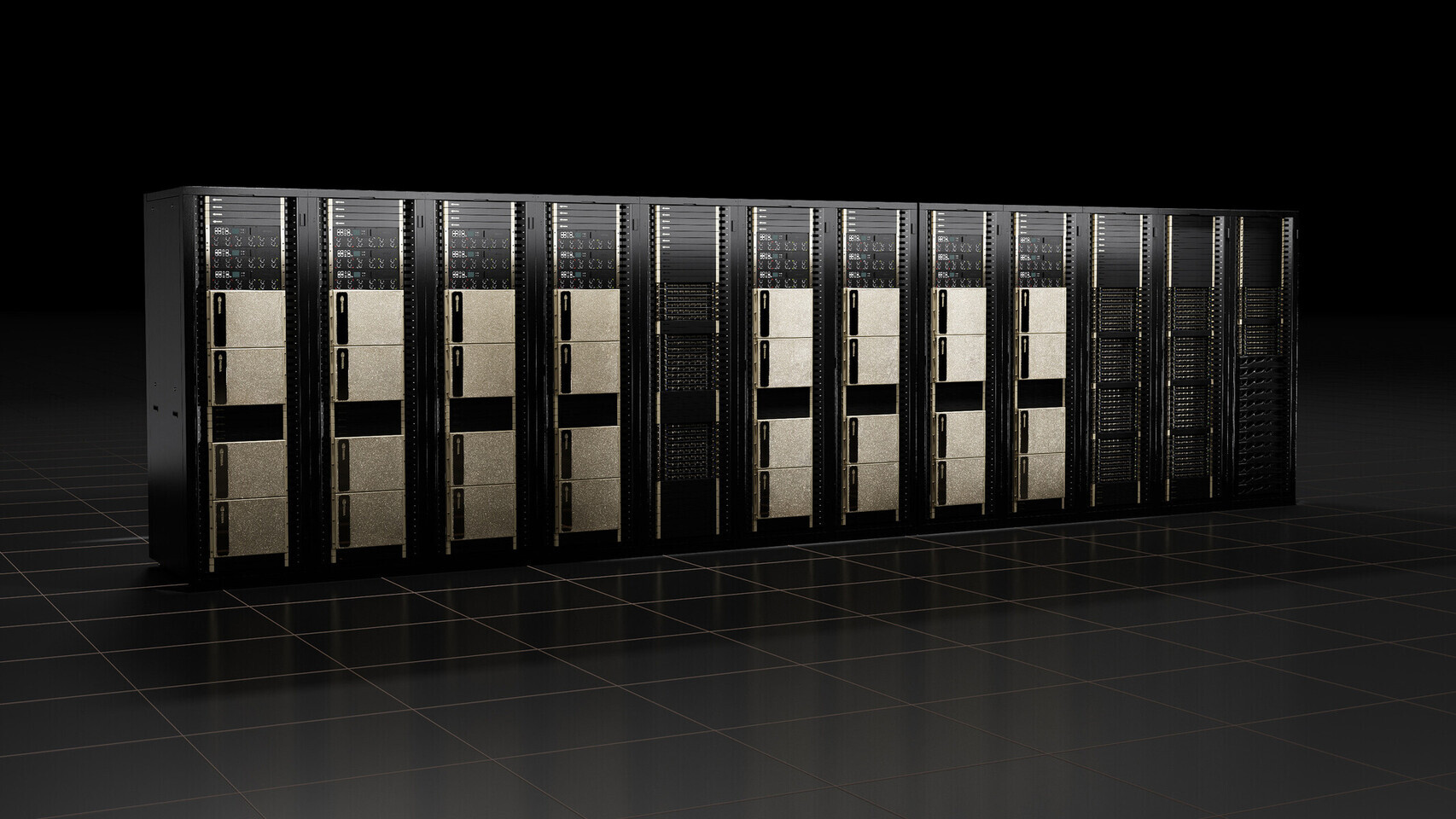
HPE Announces First Shipment of NVIDIA "Grace Blackwell" System
Hewlett Packard Enterprise announced today that it has shipped its first NVIDIA Blackwell family-based solution, the NVIDIA GB200 NVL72. This rack-scale system by HPE is designed to help service providers and large enterprises quickly deploy very large, complex AI clusters with advanced, direct liquid cooling solutions to optimize efficiency and performance. "AI service providers and large enterprise model builders are under tremendous pressure to offer scalability, extreme performance, and fast time-to-deployment," said Trish Damkroger, senior vice president and general manager of HPC & AI Infrastructure Solutions, HPE. "As builders of the world's top three fastest systems with direct liquid cooling, HPE offers customers lower cost per token training and best-in-class performance with industry-leading services expertise."
The NVIDIA GB200 NVL72 features shared-memory, low-latency architecture with the latest GPU technology designed for extremely large AI models of over a trillion parameters, in one memory space. GB200 NVL72 offers seamless integration of NVIDIA CPUs, GPUs, compute and switch trays, networking, and software, bringing together extreme performance to address heavily parallelizable workloads, like generative AI (GenAI) model training and inferencing, along with NVIDIA software applications. "Engineers, scientists and researchers need cutting-edge liquid cooling technology to keep up with increasing power and compute requirements," said Bob Pette, vice president of enterprise platforms at NVIDIA. "Building on continued collaboration between HPE and NVIDIA, HPE's first shipment of NVIDIA GB200 NVL72 will help service providers and large enterprises efficiently build, deploy and scale large AI clusters."

The NVIDIA GB200 NVL72 features shared-memory, low-latency architecture with the latest GPU technology designed for extremely large AI models of over a trillion parameters, in one memory space. GB200 NVL72 offers seamless integration of NVIDIA CPUs, GPUs, compute and switch trays, networking, and software, bringing together extreme performance to address heavily parallelizable workloads, like generative AI (GenAI) model training and inferencing, along with NVIDIA software applications. "Engineers, scientists and researchers need cutting-edge liquid cooling technology to keep up with increasing power and compute requirements," said Bob Pette, vice president of enterprise platforms at NVIDIA. "Building on continued collaboration between HPE and NVIDIA, HPE's first shipment of NVIDIA GB200 NVL72 will help service providers and large enterprises efficiently build, deploy and scale large AI clusters."


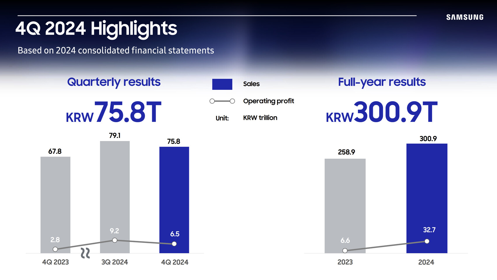
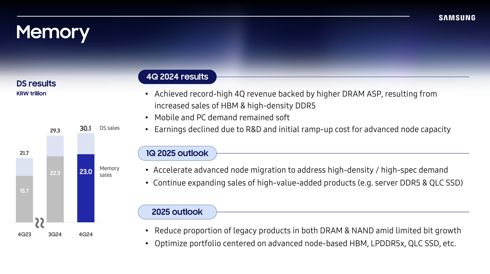
Samsung Electronics Announces Fourth Quarter and FY 2024 Results
Samsung Electronics today reported financial results for the fourth quarter and the fiscal year 2024. The Company posted KRW 75.8 trillion in consolidated revenue and KRW 6.5 trillion in operating profit in the quarter ended December 31, 2024. For the full year, it reported KRW 300.9 trillion in annual revenue and KRW 32.7 trillion in operating profit.
Although fourth quarter revenue and operating profit decreased on a quarter-on-quarter (QoQ) basis, annual revenue reached the second-highest on record, surpassed only in 2022. Meanwhile, operating profit was down KRW 2.7 trillion QoQ, due to soft market conditions especially for IT products, and an increase in expenditures including R&D. In the first quarter of 2025, while overall earnings improvement may be limited due to weakness in the semiconductors business, the Company aims to pursue growth through increased sales of smartphones with differentiated AI experiences, as well as premium products in the Device eXperience (DX) Division.


Although fourth quarter revenue and operating profit decreased on a quarter-on-quarter (QoQ) basis, annual revenue reached the second-highest on record, surpassed only in 2022. Meanwhile, operating profit was down KRW 2.7 trillion QoQ, due to soft market conditions especially for IT products, and an increase in expenditures including R&D. In the first quarter of 2025, while overall earnings improvement may be limited due to weakness in the semiconductors business, the Company aims to pursue growth through increased sales of smartphones with differentiated AI experiences, as well as premium products in the Device eXperience (DX) Division.


Numem to Showcase Next-Gen Memory Solutions at the Upcoming Chiplet Summit
Numem, an innovator focused on accelerating memory for AI workloads, will be at the upcoming Chiplet Summit to showcase its high-performance solutions. By accelerating the delivery of data via new memory subsystem designs, Numem solutions are re-architecting the hierarchy of AI memory tiers to eliminate the bottlenecks that negatively impact power and performance.
The rapid growth of AI workloads and AI Processor/GPUs are exacerbating the memory bottleneck caused by the slowing performance improvements and scalability of SRAM and DRAM - presenting a major obstacle to maximizing system performance. To overcome this, there is a pressing need for intelligent memory solutions that offer higher power efficiency and greater bandwidth, coupled with a reevaluation of traditional memory architectures.
The rapid growth of AI workloads and AI Processor/GPUs are exacerbating the memory bottleneck caused by the slowing performance improvements and scalability of SRAM and DRAM - presenting a major obstacle to maximizing system performance. To overcome this, there is a pressing need for intelligent memory solutions that offer higher power efficiency and greater bandwidth, coupled with a reevaluation of traditional memory architectures.

SK hynix Ships HBM4 Samples to NVIDIA in June, Mass Production Slated for Q3 2025
SK hynix has sped up its HBM4 development plans, according to a report from ZDNet. The company wants to start shipping HBM4 samples to NVIDIA this June, which is earlier than the original timeline. SK hynix hopes to start supplying products by the end of Q3 2025, this push likely aims to get a head start in the next-gen HBM market. To meet this sped-up schedule, SK hynix has set up a special HBM4 development team to supply NVIDIA. Industry sources indicated on January 15th that SK Hynix plans to deliver its first customer samples of HBM4 in early June this year. The company hit a big milestone when it wrapped up the HBM4 tapeout in Q4 2024, the last design step.
HBM4 marks the sixth iteration of high-bandwidth memory tech using stacked DRAM architecture. It comes after HBM3E, the current fifth-gen version, with large-scale production likely to kick off in late 2025 at the earliest. HBM4 boasts a big leap forward doubling data transfer ability with 2,048 I/O channels up from its forerunner. NVIDIA planned to use 12-layer stacked HBM4 in its 2026 "Rubin" line of powerful GPUs. However, NVIDIA has moved up its timeline for "Rubin" aiming to launch in late 2025.
HBM4 marks the sixth iteration of high-bandwidth memory tech using stacked DRAM architecture. It comes after HBM3E, the current fifth-gen version, with large-scale production likely to kick off in late 2025 at the earliest. HBM4 boasts a big leap forward doubling data transfer ability with 2,048 I/O channels up from its forerunner. NVIDIA planned to use 12-layer stacked HBM4 in its 2026 "Rubin" line of powerful GPUs. However, NVIDIA has moved up its timeline for "Rubin" aiming to launch in late 2025.

Micron Breaks Ground on New HBM Advanced Packaging Facility in Singapore
Micron Technology, Inc. (Nasdaq: MU) broke ground today on a new High-Bandwidth Memory (HBM) advanced packaging facility adjacent to the company's current facilities in Singapore. Micron marked the occasion with a ceremony attended by Gan Kim Yong, Deputy Prime Minister and Minister for Trade and Industry of Singapore, Png Cheong Boon, Chairman of the Singapore Economic Development Board, Pee Beng Kong, Executive Vice President of the Singapore Economic Development Board, and Tan Boon Khai, CEO of JTC Corporation.
The new HBM advanced packaging facility will be the first facility of its kind in Singapore. Operations for the new facility are scheduled to begin in 2026, with meaningful expansion of Micron's total advanced packaging capacity beginning in calendar 2027 to meet the demands of AI growth. The launch of this facility will further strengthen Singapore's local semiconductor ecosystem and innovation.
The new HBM advanced packaging facility will be the first facility of its kind in Singapore. Operations for the new facility are scheduled to begin in 2026, with meaningful expansion of Micron's total advanced packaging capacity beginning in calendar 2027 to meet the demands of AI growth. The launch of this facility will further strengthen Singapore's local semiconductor ecosystem and innovation.

SK hynix Showcases AI-Driven Innovations for a Sustainable Tomorrow at CES 2025
SK hynix has returned to Las Vegas for Consumer Electronics Show (CES) 2025, showcasing its latest AI memory innovations reshaping the industry. Held from January 7-10, CES 2025 brings together the brightest minds and groundbreaking technologies from the world's leading tech companies. This year, the event's theme is "Dive In," inviting attendees to immerse themselves in the next wave of technological advancement. SK hynix is emphasizing how it is driving this wave through a display of leading AI memory technologies at the SK Group exhibit. Along with SK Telecom, SKC, and SK Enmove, the company is highlighting how the Group's AI infrastructure brings about true change under the theme "Innovative AI, Sustainable Tomorrow."
Groundbreaking Memory Tech Driving Change in the AI Era
Visitors enter SK Group's exhibit through the Innovation Gate, greeted by a video of dynamic wave-inspired visuals which symbolize the power of AI. The video shows the transformation of binary data into a wave which flows through the exhibition, highlighting how data and AI drives change across industries. Continuing deeper into the exhibit, attendees make their way into the AI Data Center area, the focal point of SK hynix's display. This area features the company's transformative memory products driving progress in the AI era. Among the cutting-edge AI memory technologies on display are SK hynix's HBM, server DRAM, eSSD, CXL, and PIM products.


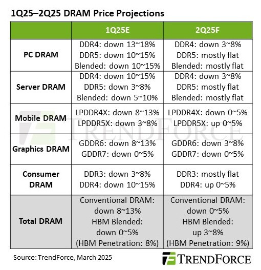
Passive Buyer Strategies Drive DRAM Contract Prices Down Across the Board in 1Q25
TrendForce's latest investigations reveal that the DRAM market is expected to face downward pricing pressure in 1Q25 as seasonal weakness aligns with sluggish consumer demand for products like smartphones. Additionally, early stockpiling by notebook manufacturers—over potential import tariffs under the Trump administration—has further exacerbated the pricing decline.
Conventional DRAM prices are projected to drop by 8% to 13%. However, if HBM products are included, the anticipated price decline will range from 0% to 5%.
Conventional DRAM prices are projected to drop by 8% to 13%. However, if HBM products are included, the anticipated price decline will range from 0% to 5%.

CXMT Achieves 80% Yield for DDR5 Chips, HBM2 Production and Capacity Expansion Underway
According to a recent Citigroup analysis, CXMT, China's domestic memory chipmaker, is demonstrating significant progress in its DDR5 production yields. The company's DDR5 yield rates had reached approximately 80%, marking a substantial improvement from its initial 50% yields when production began. This progress builds on CXMT's experience with DDR4 manufacturing, where the company has achieved yields of around 90%. The company currently operates two fab facilities in Hefei, with Fab 1 dedicated to DDR4 production on 19 nm process technology and a 100,000 wafer per month capacity. Fab 2 focuses on DDR5 production using 17 nm technology, with a current capacity of 50,000 wafers per month. CXMT's DDR5 yields could improve further to approximately 90% by the end of 2025.
Despite these improvements, CXMT faces technological challenges compared to industry leaders. The company's current production process is 19 nm for DDR4 and 17 nm for DDR5, lagging behind competitors like Samsung and SK Hynix, which manufacture 12 nm DDR5 chips. This technology gap results in higher power consumption and less favorable form factors for CXMT's products. The company primarily targets domestic Chinese smartphone and computing OEM customers. Looking ahead, CXMT plans to expand its DDR5 and HBM capabilities, with a potential additional capacity of 50,000 wafers per month at Fab 2 in 2025, if market conditions prove favorable. The company is also making progress on HBM2 development, with customer sampling underway and low-volume production expected to begin in mid-2025.

Despite these improvements, CXMT faces technological challenges compared to industry leaders. The company's current production process is 19 nm for DDR4 and 17 nm for DDR5, lagging behind competitors like Samsung and SK Hynix, which manufacture 12 nm DDR5 chips. This technology gap results in higher power consumption and less favorable form factors for CXMT's products. The company primarily targets domestic Chinese smartphone and computing OEM customers. Looking ahead, CXMT plans to expand its DDR5 and HBM capabilities, with a potential additional capacity of 50,000 wafers per month at Fab 2 in 2025, if market conditions prove favorable. The company is also making progress on HBM2 development, with customer sampling underway and low-volume production expected to begin in mid-2025.


Nanya Technology Partners With PieceMakers to Develop Customized Ultra-High-Bandwidth Memory
Nanya Technology's Board of Directors today has approved a strategic partnership with PieceMakers Technology, Inc. ("PieceMakers") to jointly develop customized ultra-high-bandwidth memory solutions. As part of the collaboration, Nanya Technology will subscribe to a cash capital increase of up to NT$ 660 million, purchasing up to 22 million common shares at NT$ 30 per share in PieceMakers. Upon completion of the capital increase, Nanya Technology is expected to acquire up to approximately 38% stakes of PieceMakers.
To meet the growing demand for high-performance memory driven by AI and edge computing, this collaboration will combine Nanya Technology's 10 nm-class DRAM innovation with PieceMakers' expertise in customized DRAM design to develop high-value, high-performance, and low-power customized ultra-high-bandwidth memory solutions, unlocking new opportunities in AI and high-performance computing markets.
To meet the growing demand for high-performance memory driven by AI and edge computing, this collaboration will combine Nanya Technology's 10 nm-class DRAM innovation with PieceMakers' expertise in customized DRAM design to develop high-value, high-performance, and low-power customized ultra-high-bandwidth memory solutions, unlocking new opportunities in AI and high-performance computing markets.
Marvell Announces Custom HBM Compute Architecture for AI Accelerators
Marvell Technology, Inc. (NASDAQ: MRVL), a leader in data infrastructure semiconductor solutions, today announced that it has pioneered a new custom HBM compute architecture that enables XPUs to achieve greater compute and memory density. The new technology is available to all of its custom silicon customers to improve the performance, efficiency and TCO of their custom XPUs. Marvell is collaborating with its cloud customers and leading HBM manufacturers, Micron, Samsung Electronics, and SK hynix to define and develop custom HBM solutions for next-generation XPUs.
HBM is a critical component integrated within the XPU using advanced 2.5D packaging technology and high-speed industry-standard interfaces. However, the scaling of XPUs is limited by the current standard interface-based architecture. The new Marvell custom HBM compute architecture introduces tailored interfaces to optimize performance, power, die size, and cost for specific XPU designs. This approach considers the compute silicon, HBM stacks, and packaging. By customizing the HBM memory subsystem, including the stack itself, Marvell is advancing customization in cloud data center infrastructure. Marvell is collaborating with major HBM makers to implement this new architecture and meet cloud data center operators' needs.

HBM is a critical component integrated within the XPU using advanced 2.5D packaging technology and high-speed industry-standard interfaces. However, the scaling of XPUs is limited by the current standard interface-based architecture. The new Marvell custom HBM compute architecture introduces tailored interfaces to optimize performance, power, die size, and cost for specific XPU designs. This approach considers the compute silicon, HBM stacks, and packaging. By customizing the HBM memory subsystem, including the stack itself, Marvell is advancing customization in cloud data center infrastructure. Marvell is collaborating with major HBM makers to implement this new architecture and meet cloud data center operators' needs.


Apr 18th, 2025 15:03 EDT
change timezone
Latest GPU Drivers
New Forum Posts
- What are you playing? (23396)
- TPU's Nostalgic Hardware Club (20256)
- Can Intel recover in DYI market anytime soon? (7)
- Spoofer Modified SMBIOS/BIOS – Need Help Restoring Original Motherboard Info (TUF GAMING B550-PLUS WiFi II) (2)
- Tried installing 576.02 - installer window disappears (20)
- GPU Pricing and Performance (14)
- Place your bets, what node will rtx 6000/RDNA 5(UDNA 1?) use (6)
- RX 9000 series GPU Owners Club (392)
- GPU Database (300)
- Drives fail to work with Rufus Windows TO GO (2)
Popular Reviews
- ASUS GeForce RTX 5060 Ti TUF OC 16 GB Review
- NVIDIA GeForce RTX 5060 Ti PCI-Express x8 Scaling
- Palit GeForce RTX 5060 Ti Infinity 3 16 GB Review
- G.SKILL Trident Z5 NEO RGB DDR5-6000 32 GB CL26 Review - AMD EXPO
- ASUS GeForce RTX 5060 Ti Prime OC 16 GB Review
- MSI GeForce RTX 5060 Ti Gaming OC 16 GB Review
- Zotac GeForce RTX 5060 Ti AMP 16 GB Review
- Teevolution Terra Pro Review
- MSI GeForce RTX 5060 Ti Gaming Trio OC 16 GB Review
- ASUS GeForce RTX 5080 TUF OC Review
Controversial News Posts
- NVIDIA GeForce RTX 5060 Ti 16 GB SKU Likely Launching at $499, According to Supply Chain Leak (182)
- NVIDIA Sends MSRP Numbers to Partners: GeForce RTX 5060 Ti 8 GB at $379, RTX 5060 Ti 16 GB at $429 (127)
- Nintendo Confirms That Switch 2 Joy-Cons Will Not Utilize Hall Effect Stick Technology (105)
- Over 200,000 Sold Radeon RX 9070 and RX 9070 XT GPUs? AMD Says No Number was Given (100)
- Nintendo Switch 2 Launches June 5 at $449.99 with New Hardware and Games (99)
- NVIDIA Launches GeForce RTX 5060 Series, Beginning with RTX 5060 Ti This Week (98)
- Sony Increases the PS5 Pricing in EMEA and ANZ by Around 25 Percent (85)
- NVIDIA PhysX and Flow Made Fully Open-Source (77)