News Posts matching #HBM

Return to Keyword Browsing

SiPearl to Manufacture its 72-Core Rhea HPC SoC at TSMC Facilities

SiPearl has this week announced their collaboration with Open-Silicon Research, the India-based entity of OpenFive, to produce the next-generation SoC designed for HPC purposes. SiPearl is a part of the European Processor Initiative (EPI) team and is responsible for designing the SoC itself that is supposed to be a base for the European exascale supercomputer. In the partnership with Open-Silicon Research, SiPearl expects to get a service that will integrate all the IP blocks and help with the tape out of the chip once it is done. There is a deadline set for the year 2023, however, both companies expect the chip to get shipped by Q4 of 2022.

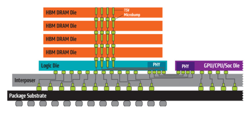
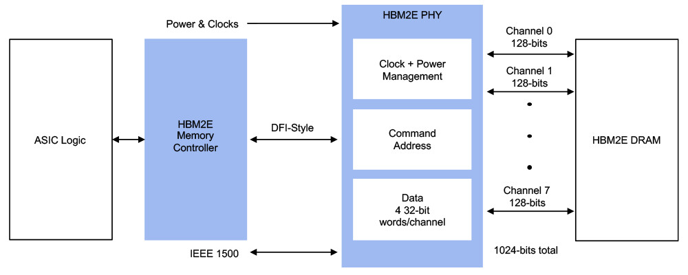
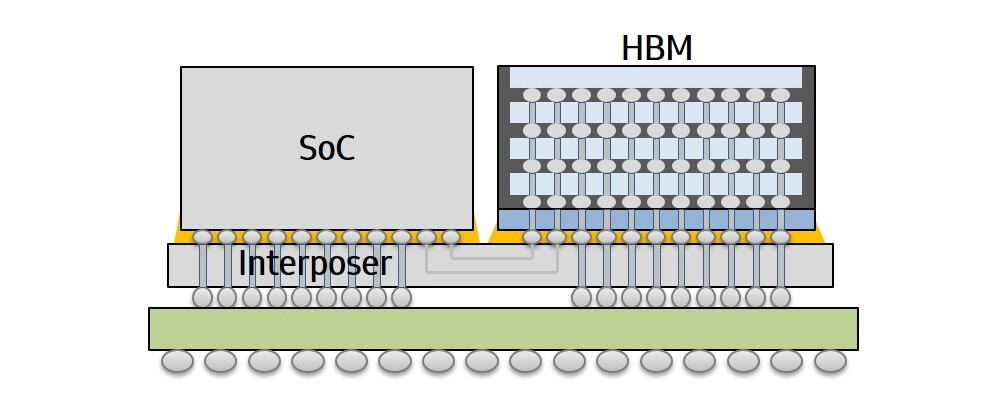
When it comes to details of the SoC, it is called Rhea and it will be a 72-core Arm ISA based processor with Neoverse Zeus cores interconnected by a mesh. There are going to be 68 mesh network L3 cache slices in between all of the cores. All of that will be manufactured using TSMC's 6 nm extreme ultraviolet lithography (EUV) technology for silicon manufacturing. The Rhea SoC design will utilize 2.5D packaging with many IP blocks stitched together and HBM2E memory present on the die. It is unknown exactly what configuration of HBM2E is going to be present. The system will also see support for DDR5 memory and thus enable two-level system memory by combining HBM and DDR. We are excited to see how the final product looks like and now we wait for more updates on the project.

Intel Confirms HBM is Supported on Sapphire Rapids Xeons

Intel has just released its "Architecture Instruction Set Extensions and Future Features Programming Reference" manual, which serves the purpose of providing the developers' information about Intel's upcoming hardware additions which developers can utilize later on. Today, thanks to the @InstLatX64 on Twitter we have information that Intel is bringing on-package High Bandwidth Memory (HBM) solution to its next-generation Sapphire Rapids Xeon processors. Specifically, there are two instructions mentioned: 0220H - HBM command/address parity error and 0221H - HBM data parity error. Both instructions are there to address data errors in HBM so the CPU operates with correct data.

The addition of HBM is just one of the many new technologies Sapphire Rapids brings. The platform is supposedly going to bring many new technologies like an eight-channel DDR5 memory controller enriched with Intel's Data Streaming Accelerator (DSA). To connect to all of the external accelerators, the platform uses PCIe 5.0 protocol paired with CXL 1.1 standard to enable cache coherency in the system. And as a reminder, this would not be the first time we see a server CPU use HBM. Fujitsu has developed an A64FX processor with 48 cores and HBM memory, and it is powering today's most powerful supercomputer - Fugaku. That is showing how much can a processor get improved by adding a faster memory on-board. We are waiting to see how Intel manages to play it out and what we end up seeing on the market when Sapphire Rapids is delivered.

BittWare Launches IA-840F with Intel Agilex FPGA and Support for oneAPI

BittWare, a Molex company, today unveiled the IA-840F, the company's first Intel Agilex -based FPGA card designed to deliver significant performance-per-watt improvements for next-generation data center, networking and edge compute workloads. Agilex FPGAs deliver up to 40% higher performance or up to 40% lower power, depending on application requirements. BittWare maximized I/O features using the Agilex chip's unique tiling architecture with dual QSFP-DDs (4× 100G), PCIe Gen4 x16, and three MCIO expansion ports for diverse applications. BittWare also announced support for Intel oneAPI, which enables an abstracted development flow for dramatically simplified code re-use across multiple architectures.

"Modern data center workloads are incredibly diverse, requiring customers to implement a mix of scalar, vector, matrix and spatial architectures," said Craig Petrie, vice president of marketing for BittWare. "The IA-840F ensures that customers can quickly and easily exploit the advanced features of the Intel Agilex FPGA. For those customers who prefer to develop FPGA applications at an abstracted level, we are including support for oneAPI. This new unified software programming environment allows customers to program the Agilex FPGA from a single code base with native high-level language performance across architectures."

SK hynix Inc. Reports Third Quarter 2020 Results

SK hynix Inc. today announced financial results for its third quarter 2020 ended on September 30, 2020. The consolidated revenue of third quarter 2020 was 8.129 trillion won while the operating profit amounted to 1.3 trillion won, and the net income 1.078 trillion won. Operating margin for the quarter was 16% and net margin was 13%.

Despite the Company saw the recovery of mobile DRAM demand in the quarter, both the revenue and operating profit decreased by 6% and 33% quarter-over-quarter (QoQ) respectively, as the server DRAM and SSD demands weakened, and the overall semiconductor memory price flow turned downwards in the quarter. For DRAM, SK hynix proactively responded to rising demands of mobile and graphics DRAM, and the expansion of consumer electronics DRAM demand as well. As a result, in spite of decreased server DRAM demand, the Company's DRAM bit shipment in the quarter still increased by 4% QoQ. However, due to the unfavorable price of server DRAM and other certain DRAM products, the average selling price decreased by 7% QoQ.

TSMC to Enter Mass Production of 6th Generation CoWoS Packaging in 2023, up to 12 HBM Stacks

TSMC, the world's leading semiconductor manufacturing company, is rumored to start production of its 6th generation Chip-on-Wafer-on-Substrate (CoWoS) packaging technology. As the silicon scaling is getting ever so challenging, the manufacturers have to come up with a way to get as much performance as possible. That is where TSMC's CoWoS and other chiplet technologies come. They allow designers to integrate many integrated circuits on a single package, making for a cheaper overall product compared to if the product used one big die. So what is so special about 6th generation CoWoS technology from TSMC, you might wonder. The new generation is said to enable a massive 12 stacks of HBM memory on a package. You are reading that right. Imagine if each stack would be an HBM2E variant with 16 GB capacity that would be 192 GB of memory on the package present. Of course, that would be a very expensive chip to manufacture, however, it is just a showcase of what the technology could achieve.

Update 16:44 UTC—TheEnglish DigiTimes report indicates that this technology is expected to see mass production in 2023.

AMD Big Navi GPU Features Infinity Cache?

As we are nearing the launch of AMD's highly hyped, next-generation RDNA 2 GPU codenamed "Big Navi", we are seeing more details emerge and crawl their way to us. We already got some rumors suggesting that this card is supposedly going to be called AMD Radeon RX 6900 and it is going to be AMD's top offering. Using a 256-bit bus with 16 GB of GDDR6 memory, the GPU will not use any type of HBM memory, which has historically been rather pricey. Instead, it looks like AMD will compensate for a smaller bus with a new technology it has developed. Thanks to the new findings on Justia Trademarks website by @momomo_us, we have information about the alleged "infinity cache" technology the new GPU uses.

It is reported by VideoCardz that the internal name for this technology is not Infinity Cache, however, it seems that AMD could have changed it recently. What does exactly you might wonder? Well, it is a bit of a mystery for now. What it could be, is a new cache technology which would allow for L1 GPU cache sharing across the cores, or some connection between the caches found across the whole GPU unit. This information should be taken with a grain of salt, as we are yet to see what this technology does and how it works, when AMD announces their new GPU on October 28th.

Rambus Advances HBM2E Performance to 4.0 Gbps for AI/ML Training Applications

Rambus Inc. (NASDAQ: RMBS), a premier silicon IP and chip provider making data faster and safer, today announced it has achieved a record 4 Gbps performance with the Rambus HBM2E memory interface solution consisting of a fully-integrated PHY and controller. Paired with the industry's fastest HBM2E DRAM from SK hynix operating at 3.6 Gbps, the solution can deliver 460 GB/s of bandwidth from a single HBM2E device. This performance meets the terabyte-scale bandwidth needs of accelerators targeting the most demanding AI/ML training and high-performance computing (HPC) applications.

"With this achievement by Rambus, designers of AI and HPC systems can now implement systems using the world's fastest HBM2E DRAM running at 3.6 Gbps from SK hynix," said Uksong Kang, vice president of product planning at SK hynix. "In July, we announced full-scale mass-production of HBM2E for state-of-the-art computing applications demanding the highest bandwidth available."

NVIDIA Tesla A100 GPU Pictured

Thanks to the sources of VideoCardz, we now have the first picture of the next-generation NVIDIA Tesla A100 graphics card. Designed for computing oriented applications, the Tesla A100 is a socketed GPU designed for NVIDIA's proprietary SXM socket. In a post few days ago, we were suspecting that you might be able to fit the Tesla A100 GPU in the socket of the previous Volta V100 GPUs as it is a similar SXM socket. However, the mounting holes have been re-arranged and this one requires a new socket/motherboard. The Tesla A100 GPU is based on GA100 GPU die, which we don't know specifications of. From the picture, we can only see that there is one very big die attached to six HBM modules, most likely HBM2E. Besides that everything else is unknown. More details are expected to be announced today at the GTC 2020 digital keynote.
NVIDIA Tesla A100

Fujitsu Completes Delivery of Fugaku Supercomputer

Fujitsu has today officially completed the delivery of the Fugaku supercomputer to the Riken scientific research institute of Japan. This is a big accomplishment as the current COVID-19 pandemic has delayed many happenings in the industry. However, Fujitsu managed to play around that and deliver the supercomputer on time. The last of 400 racks needed for the Fugaku supercomputer was delivered today, on May 13th, as it was originally planned. The supercomputer is supposed to be fully operational starting on the physical year of 2021, where the installation and setup will be done before.

As a reminder, the Fugaku is an Arm-based supercomputer consisting out of 150 thousand A64FX CPUs. These CPUs are custom made processors by Fujitsu based on Arm v8.2 ISA, and they feature 48 cores built on TSMC 7 nm node and running above 2 GHz. Packing 8.786 billion transistors, this monster chips use HBM2 memory instead of a regular DDR memory interface. Recently, a prototype of the Fugaku supercomputer was submitted to the Top500 supercomputer list and it came on top for being the most energy-efficient of all, meaning that it will be as energy efficient as it will be fast. Speculations are that it will have around 400 PetaFlops of general compute power for Dual-Precision workloads, however, for the specific artificial intelligence applications, it should achieve ExaFLOP performance target.
K SuperComputer

Micron to Launch HBM2 Memory This Year

Micron Technologies, in the latest earnings report, announced that they will start shipping High-Bandwidth Memory 2 (HBM2) DRAM. Used for high-performance graphics cards, server processors and all kinds of processors, HBM2 memory is wanted and relatively expensive solution, however, when Micron enters the market of its manufacturing, prices, and the market should adjust for the new player. Previously, only SK-Hynix and Samsung were manufacturing the HBM2 DRAM, however, Micron will join them and they will again form a "big-three" pact that dominates the memory market.

Up until now, Micron used to lay all hopes on its proprietary Hybrid Memory Cube (HMC) DRAM type, which didn't gain much traction from customers and it never really took off. Only a few rare products used it, as Fujitsu SPARC64 XIfx CPU used in Fujitsu PRIMEHPC FX100 supercomputer introduced in 2015. Micron announced to suspend works on HMC in 2018 and decided to devote their efforts to GDDR6 and HBM development. So, as a result, we are seeing that they will launch HBM2 DRAM products sometime this year.
Micron HMC High-Bandwidth Memory

Rambus Designs HBM2E Controller and PHY

Rambus, a maker of various Interface IP solutions, today announced the latest addition to its high-speed memory interface IP product portfolio in form of High Bandwidth Memory 2E (HBM2E) controller and physical layer (PHY) IP solution. The two IPs are enabling customers to completely integrate the HBM2E memory into their products, given that Rambus provides a complete solution for controlling and interfacing the memory. The design that Ramus offers can support for 12-high DRAM stacks of up to 24 Gb devices, making for up to 36 GB of memory per 3D stack. This single 3D stack is capable of delivering 3.2 Gbps over a 1024-bit wide interface, delivering 410 GB/s of bandwidth per stack.

The HBM2E controller core is DFI 3.1 compatible and has support for logic interfaces like AXI, OCP, or a custom one, so the customer can choose a way to integrate this core in their design. With a purchase of their HBM2E IP, Rambus will provide source code written in Hardware Description Language (HDL) and GDSII file containing the layout of the interface.

Samsung Launches 3rd-Generation "Flashbolt" HBM2E Memory

Samsung Electronics, the world leader in advanced memory technology, today announced the market launch of 'Flashbolt', its third-generation High Bandwidth Memory 2E (HBM2E). The new 16-gigabyte (GB) HBM2E is uniquely suited to maximize high performance computing (HPC) systems and help system manufacturers to advance their supercomputers, AI-driven data analytics and state-of-the-art graphics systems in a timely manner.

"With the introduction of the highest performing DRAM available today, we are taking a critical step to enhance our role as the leading innovator in the fast-growing premium memory market," said Cheol Choi, executive vice president of Memory Sales & Marketing at Samsung Electronics. "Samsung will continue to deliver on its commitment to bring truly differentiated solutions as we reinforce our edge in the global memory marketplace."

Europe Readies its First Prototype of Custom HPC Processor

European Processor Initiative (EPI) is a Europe's project to kickstart a homegrown development of custom processors tailored towards different usage models that the European Union might need. The first task of EPI is to create a custom processor for high-performance computing applications like machine learning, and the chip prototypes are already on their way. The EPI chairman of the board Jean-Marc Denis recently spoke to the Next Platform and confirmed some information regarding the processor design goals and the timeframe of launch.

Supposed to be manufactured on TSMC's 6 nm EUV (TSMC N6 EUV) technology, the EPI processor will tape-out at the end of 2020 or the beginning of 2021, and it is going to be heterogeneous. That means that on its 2.5D die, many different IPs will be present. The processor will use a custom ARM CPU, based on a "Zeus" iteration of Neoverese server core, meant for general-purpose computation tasks like running the OS. When it comes to the special-purpose chips, EPI will incorporate a chip named Titan - a RISC-V based processor that uses vector and tensor processing units to compute AI tasks. The Titan will use every new standard for AI processing, including FP32, FP64, INT8, and bfloat16. The system will use HBM memory allocated to the Titan processor, have DDR5 links for the CPU, and feature PCIe 5.0 for the inner connection.

Samsung Starts Production of AI Chips for Baidu

Baidu, a leading Chinese-language Internet search provider, and Samsung Electronics, a world leader in advanced semiconductor technology, today announced that Baidu's first cloud-to-edge AI accelerator, Baidu KUNLUN, has completed its development and will be mass-produced early next year. Baidu KUNLUN chip is built on the company's advanced XPU, a home-grown neural processor architecture for cloud, edge, and AI, as well as Samsung's 14-nanometer (nm) process technology with its I-Cube (Interposer-Cube) package solution.

The chip offers 512 gigabytes per second (GBps) memory bandwidth and supplies up to 260 Tera operations per second (TOPS) at 150 watts. In addition, the new chip allows Ernie, a pre-training model for natural language processing, to infer three times faster than the conventional GPU/FPGA-accelerating model. Leveraging the chip's limit-pushing computing power and power efficiency, Baidu can effectively support a wide variety of functions including large-scale AI workloads, such as search ranking, speech recognition, image processing, natural language processing, autonomous driving, and deep learning platforms like PaddlePaddle.

Moore's Law - Is it Really Dead ?

"Moore's Law" is a term coined in 1965 by Gordon Moore, who presented a paper which predicts that semiconductor scaling will allow integrated circuits to feature twice as many transistors present per same area as opposed to a chip manufactured two years ago. That means we could get same performance at half the power than the previous chip, or double the performance at same power/price in only two years time. Today we'll investigate if Moore's Law stayed true to its cause over the years and how much longer can it keep going.

Intel Ships First 10nm Agilex FPGAs

Intel today announced that it has begun shipments of the first Intel Agilex field programmable gate arrays (FPGAs) to early access program customers. Participants in the early access program include Colorado Engineering Inc., Mantaro Networks, Microsoft and Silicom. These customers are using Agilex FPGAs to develop advanced solutions for networking, 5G and accelerated data analytics.

"The Intel Agilex FPGA product family leverages the breadth of Intel innovation and technology leadership, including architecture, packaging, process technology, developer tools and a fast path to power reduction with eASIC technology. These unmatched assets enable new levels of heterogeneous computing, system integration and processor connectivity and will be the first 10nm FPGA to provide cache-coherent and low latency connectivity to Intel Xeon processors with the upcoming Compute Express Link," said Dan McNamara, Intel senior vice president and general manager of the Networking and Custom Logic Group.

Intel Driving Data-Centric World with New 10nm Intel Agilex FPGA Family

Intel announced today a brand-new product family, the Intel Agilex FPGA. This new family of field programmable gate arrays (FPGA) will provide customized solutions to address the unique data-centric business challenges across embedded, network and data center markets. "The race to solve data-centric problems requires agile and flexible solutions that can move, store and process data efficiently. Intel Agilex FPGAs deliver customized connectivity and acceleration while delivering much needed improvements in performance and power for diverse workloads," said Dan McNamara, Intel senior vice president, Programmable Solutions Group.

Customers need solutions that can aggregate and process increasing amounts of data traffic to enable transformative applications in emerging, data-driven industries like edge computing, networking and cloud. Whether it's through edge analytics for low-latency processing, virtualized network functions to improve performance, or data center acceleration for greater efficiency, Intel Agilex FPGAs are built to deliver customized solutions for applications from the edge to the cloud. Advances in artificial intelligence (AI) analytics at the edge, network and the cloud are compelling hardware systems to cope with evolving standards, support varying AI workloads, and integrate multiple functions. Intel Agilex FPGAs provide the flexibility and agility required to meet these challenges and deliver gains in performance and power.

JEDEC Updates Groundbreaking High Bandwidth Memory (HBM) Standard

JEDEC Solid State Technology Association, the global leader in the development of standards for the microelectronics industry, today announced the publication of an update to JESD235 High Bandwidth Memory (HBM) DRAM standard. HBM DRAM is used in Graphics, High Performance Computing, Server, Networking and Client applications where peak bandwidth, bandwidth per watt, and capacity per area are valued metrics to a solution's success in the market. The standard was developed and updated with support from leading GPU and CPU developers to extend the system bandwidth growth curve beyond levels supported by traditional discrete packaged memory. JESD235B is available for download from the JEDEC website.

JEDEC standard JESD235B for HBM leverages Wide I/O and TSV technologies to support densities up to 24 GB per device at speeds up to 307 GB/s. This bandwidth is delivered across a 1024-bit wide device interface that is divided into 8 independent channels on each DRAM stack. The standard can support 2-high, 4-high, 8-high, and 12-high TSV stacks of DRAM at full bandwidth to allow systems flexibility on capacity requirements from 1 GB - 24 GB per stack.

Samsung Unveils 256-Gigabyte 3DS DDR4 RDIMM, Other Datacenter Innovations

Samsung Electronics, a world leader in advanced semiconductor technology, today announced several groundbreaking additions to its comprehensive semiconductor ecosystem that encompass next-generation technologies in foundry as well as NAND flash, SSD (solid state drive) and DRAM. Together, these developments mark a giant step forward for Samsung's semiconductor business.

"Samsung's technology leadership and product breadth are unparalleled," said JS Choi, President, Samsung Semiconductor, Inc. "Bringing 7 nm EUV into production is an incredible achievement. Also, the announcements of SmartSSD and 256GB 3DS RDIMM represent performance and capacity breakthroughs that will continue to push compute boundaries. Together, these additions to Samsung's comprehensive technology ecosystem will power the next generation of datacenters, high-performance computing (HPC), enterprise, artificial intelligence (AI) and emerging applications."

Micron Announces Its Initial Launch Partner Status for NVIDIA RTX 20-Series GDDR6 Implementation

Memory subsystems are an important part of graphics workloads, and both AMD and NVIDIA have always been looking to cross the cutting-edge of tech in both GPU production and memory fabrication technologies. AMD has been hitching itself to the HBM bandwagon with much more fervor than NVIDIA, albeit with somewhat lukewarm results - at least from a consumer, gaming GPU perspective. NVIDIA has been more cautious: lock HBM's higher costs and lower availability to higher-margin products that can leverage the additional bandwidth, and leave GDDR to muscle its way through consumer products - a strategy that has likely helped in keeping BOM costs for its graphics cards relatively low.

As it stands, Micron was the only company with both the roadmap and production volume to be NVIDIA's partner in launching the RTX 20-series, with products above (and including) the GTX 2070 all carrying the new high-performance memory subsystem. Micron has already announced GDDR6 memory as a product back in 2017, with sampling by the beginning of 2018 and mass volume production by June - just enough time to spool up a nice inventory for new, shiny graphics cards to come out in September. Of course, this ramp-up and initial Micron leadership doesn't mean they will be the only suppliers for NVIDIA - however, it's safe to say they'll be the most relevant one for at least a good while.

AMD Announces Dual-Vega Radeon Pro V340 for High-Density Computing

AMD today at VMworld in Las Vegas announced their new, high-density computing, dual-GPU Radeon Pro V340 accelerator. This graphics card (or maybe accelerator) is based on the same Vega that makes AMD's consumer graphics card lineup, and crams its dual GPUs into a single card with a dual-slot design. 32 GB of second-generation Error Correcting Code (ECC) high-bandwidth memory (HBM) greases the wheels for the gargantuan amounts of data these accelerators are meant to crunch and power through, even as media processing requirements go through the roof.

Xilinx Unveils Their Revolutionary Adaptive Compute Acceleration Platform

Xilinx, Inc., the leader in adaptive and intelligent computing, today announced a new breakthrough product category called adaptive compute acceleration platform (ACAP) that goes far beyond the capabilities of an FPGA. An ACAP is a highly integrated multi-core heterogeneous compute platform that can be changed at the hardware level to adapt to the needs of a wide range of applications and workloads. An ACAP's adaptability, which can be done dynamically during operation, delivers levels of performance and performance per-watt that is unmatched by CPUs or GPUs.

An ACAP is ideally suited to accelerate a broad set of applications in the emerging era of big data and artificial intelligence. These include: video transcoding, database, data compression, search, AI inference, genomics, machine vision, computational storage and network acceleration. Software and hardware developers will be able to design ACAP-based products for end point, edge and cloud applications. The first ACAP product family, codenamed "Everest," will be developed in TSMC 7nm process technology and will tape out later this year.

NVIDIA to Unveil "Ampere" Based GeForce Product Next Month

NVIDIA prepares to make its annual tech expo, the 2018 Graphics Technology Conference (GTC) action-packed. The company already surprised us with its next-generation "Volta" architecture based TITAN V graphics card priced at 3 grand; and is working to cash in on the crypto-currency wave and ease pressure on consumer graphics card inventories by designing highly optimized mining accelerators under the new Turing brand. There's now talk that NVIDIA could pole-vault launch of the "Volta" architecture for the consumer-space; by unveiling a GeForce graphics card based on its succeeding architecture, "Ampere."

The oldest reports of NVIDIA unveiling "Ampere" date back to November 2017. At the time it was expected that NVIDIA will only share some PR blurbs on some of the key features it brings to the table, or at best, unveil a specialized (non-gaming) silicon, such as a Drive or machine-learning chip. An Expreview report points at the possibility of a GeForce product, one that you can buy in your friendly neighborhood PC store and play games with. The "Ampere" based GPU will still be based on the 12 nanometer silicon fabrication process at TSMC, and is unlikely to be a big halo chip with exotic HBM stacks. Why NVIDIA chose to leapfrog is uncertain. GTC gets underway late-March.

Intel Announces "Coffee Lake" + AMD "Vega" Multi-chip Modules

Rumors of the unthinkable silicon collaboration between Intel and AMD are true, as Intel announced its first multi-chip module (MCM), which combines a 14 nm Core "Coffee Lake-H" CPU die, with a specialized 14 nm GPU die by AMD, based on the "Vega" architecture. This GPU die has its own HBM2 memory stack over a 1024-bit wide memory bus. Unlike on the AMD "Vega 10" and "Fiji" MCMs, in which a silicon interposer is used to connect the GPU die to the memory stacks, Intel deployed the Embedded Multi-Die Interconnect Bridge (EMIB), a high-density substrate-level wiring. The CPU and GPU dies talk to each other over PCI-Express gen 3.0, wired through the package substrate.

This multi-chip module, with a tiny Z-height, significantly reduces the board footprint of the CPU + discrete graphics implementation, when compared to having separate CPU and GPU packages with the GPU having discrete GDDR memory chips, and enables a new breed of ultra portable notebooks that pack a solid graphics muscle. The MCM should enable devices as thin as 11 mm. The specifications of the CPU and dGPU dies remain under the wraps. The first devices with these MCMs will launch by Q1 2018.
A video presentation follows.

AMD "Navi" GPU by Q3-2018: Report

AMD is reportedly accelerating launch of its first GPU architecture built on the 7 nanometer process, codenamed "Navi." Graphics cards based on the first implementation of "Navi" could launch as early as by Q3-2018 (between July and September). Besides IPC increments with its core number-crunching machinery, "Navi" will introduce a slew of memory and GPU virtualization technologies.

AMD will take its multi-chip module (MCM) approach of building high-performance GPUs a step further, by placing multiple GPU dies with their HBM stacks on a single package. The company could leverage its InfinityFabric as a high-bandwidth interconnect between the GPU dies (dubbed "GPU module"), with an I/O controller die interfacing the MCM with the host machine. With multi-GPU on the decline for games, it remains to be seen how those multiple GPU modules are visible to the operating system. In the run up to "Navi," AMD could give its current "Vega" architecture a refresh on a refined 14 nm+ process, to increase clock speeds.
Return to Keyword Browsing
Jul 14th, 2025 15:39 CDT change timezone

New Forum Posts

Popular Reviews

TPU on YouTube

Controversial News Posts