Tuesday, February 4th 2020

Samsung Launches 3rd-Generation "Flashbolt" HBM2E Memory
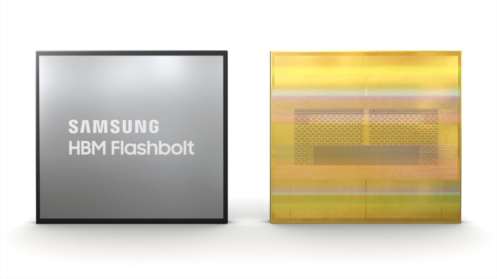
Samsung Electronics, the world leader in advanced memory technology, today announced the market launch of 'Flashbolt', its third-generation High Bandwidth Memory 2E (HBM2E). The new 16-gigabyte (GB) HBM2E is uniquely suited to maximize high performance computing (HPC) systems and help system manufacturers to advance their supercomputers, AI-driven data analytics and state-of-the-art graphics systems in a timely manner.
"With the introduction of the highest performing DRAM available today, we are taking a critical step to enhance our role as the leading innovator in the fast-growing premium memory market," said Cheol Choi, executive vice president of Memory Sales & Marketing at Samsung Electronics. "Samsung will continue to deliver on its commitment to bring truly differentiated solutions as we reinforce our edge in the global memory marketplace." Ready to deliver twice the capacity of the previous-generation 8 GB HBM2 'Aquabolt', the new Flashbolt also sharply increases performance and power efficiency to significantly improve next-generation computing systems. The 16 GB capacity is achieved by vertically stacking eight layers of 10 nm-class (1y) 16-gigabit (Gb) DRAM dies on top of a buffer chip. This HBM2E package is then interconnected in a precise arrangement of more than 40,000 'through silicon via' (TSV) microbumps, with each 16Gb die containing over 5,600 of these microscopic holes.
Samsung's Flashbolt provides a highly reliable data transfer speed of 3.2 gigabits per second (Gbps) by leveraging a proprietary optimized circuit design for signal transmission, while offering a memory bandwidth of 410 GB/s per stack. Samsung's HBM2E can also attain a transfer speed of 4.2 Gbps, the maximum tested data rate to date, enabling up to a 538 GB/s bandwidth per stack in certain future applications. This would represent a 1.75x enhancement over Aquabolt's 307 GB/s.
Samsung expects to begin volume production during the first half of this year. The company will continue providing its second-generation Aquabolt lineup while expanding its third-generation Flashbolt offering, and will further strengthen collaborations with ecosystem partners in next-generation systems as it accelerates the transition to HBM solutions throughout the premium memory market.
"With the introduction of the highest performing DRAM available today, we are taking a critical step to enhance our role as the leading innovator in the fast-growing premium memory market," said Cheol Choi, executive vice president of Memory Sales & Marketing at Samsung Electronics. "Samsung will continue to deliver on its commitment to bring truly differentiated solutions as we reinforce our edge in the global memory marketplace."
Samsung's Flashbolt provides a highly reliable data transfer speed of 3.2 gigabits per second (Gbps) by leveraging a proprietary optimized circuit design for signal transmission, while offering a memory bandwidth of 410 GB/s per stack. Samsung's HBM2E can also attain a transfer speed of 4.2 Gbps, the maximum tested data rate to date, enabling up to a 538 GB/s bandwidth per stack in certain future applications. This would represent a 1.75x enhancement over Aquabolt's 307 GB/s.
Samsung expects to begin volume production during the first half of this year. The company will continue providing its second-generation Aquabolt lineup while expanding its third-generation Flashbolt offering, and will further strengthen collaborations with ecosystem partners in next-generation systems as it accelerates the transition to HBM solutions throughout the premium memory market.
13 Comments on Samsung Launches 3rd-Generation "Flashbolt" HBM2E Memory
Where is second generation HBM2E GPU?
Where is third generation HBM2E GPU?
It'd be even better if AMD is able to pair this as "onboard RAM" onto an APU; supporting the iGPU portion, but maybe also serving as L4 cache/RAM when using light workloads or even when plugging in a dedicated GPU.
And if it proves cheap enough around 3rd Gen Navi, maybe have it standard on the GPU stack starting at the mid-range "7700~7950 XT" GPUs, if not pushing it all the way up and down the stack proper (ie "7500 to 7950 XT").
This looks like exciting stuff.