Thursday, May 14th 2020

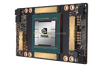
NVIDIA Tesla A100 GPU Pictured
Thanks to the sources of VideoCardz, we now have the first picture of the next-generation NVIDIA Tesla A100 graphics card. Designed for computing oriented applications, the Tesla A100 is a socketed GPU designed for NVIDIA's proprietary SXM socket. In a post few days ago, we were suspecting that you might be able to fit the Tesla A100 GPU in the socket of the previous Volta V100 GPUs as it is a similar SXM socket. However, the mounting holes have been re-arranged and this one requires a new socket/motherboard. The Tesla A100 GPU is based on GA100 GPU die, which we don't know specifications of. From the picture, we can only see that there is one very big die attached to six HBM modules, most likely HBM2E. Besides that everything else is unknown. More details are expected to be announced today at the GTC 2020 digital keynote.
Source:
VideoCardz

6 Comments on NVIDIA Tesla A100 GPU Pictured
www.techpowerup.com/gpu-specs/nvidia-ga100.g931