Thursday, September 10th 2020
Rambus Advances HBM2E Performance to 4.0 Gbps for AI/ML Training Applications
Rambus Inc. (NASDAQ: RMBS), a premier silicon IP and chip provider making data faster and safer, today announced it has achieved a record 4 Gbps performance with the Rambus HBM2E memory interface solution consisting of a fully-integrated PHY and controller. Paired with the industry's fastest HBM2E DRAM from SK hynix operating at 3.6 Gbps, the solution can deliver 460 GB/s of bandwidth from a single HBM2E device. This performance meets the terabyte-scale bandwidth needs of accelerators targeting the most demanding AI/ML training and high-performance computing (HPC) applications.
"With this achievement by Rambus, designers of AI and HPC systems can now implement systems using the world's fastest HBM2E DRAM running at 3.6 Gbps from SK hynix," said Uksong Kang, vice president of product planning at SK hynix. "In July, we announced full-scale mass-production of HBM2E for state-of-the-art computing applications demanding the highest bandwidth available."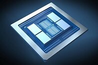
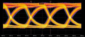 The fully-integrated, production-ready Rambus HBM2E memory subsystem runs at 4 Gbps without PHY voltage overdrive. Rambus teamed with SK hynix and Alchip to implement the HBM2E 2.5D system to validate in silicon the Rambus HBM2E PHY and Memory Controller IP using TSMC's N7 process and CoWoS (Chip-on-Wafer-on-Substrate) advanced packaging technologies. Co-designing with the engineering team from Rambus, Alchip led the interposer and package substrate design.
"This advancement of Rambus and its partners, using TSMC's advanced process and packaging technologies, is another important achievement of our ongoing collaboration with Rambus," said Suk Lee, senior director of the Design Infrastructure Management Division at TSMC. "We look forward to a continued partnership with Rambus to enable the highest performance in AI/ML and HPC applications."
"Alchip brought a demonstrated track record of success in 7nm and 2.5D package design to this initiative," said Johnny Shen, CEO of Alchip Technologies. "We're extremely proud of our contributions to Rambus' breakthrough achievement."
Rambus has 30 years of high-speed memory design applied to the most demanding computing applications. Its renowned signal integrity expertise was key to achieving an HBM2E memory interface capable of 4 Gbps operation. This raises a new benchmark for meeting the insatiable bandwidth requirements of AI/ML training.
"With silicon operation up to 4 Gbps, designers can future-proof their HBM2E implementations and can be confident of ample margin for 3.6 Gbps designs," said Matthew Jones, senior director and general manager of IP cores at Rambus. "As part of every customer engagement, Rambus provides reference designs for the 2.5D package and interposer to ensure first-time right implementations for mission-critical AI/ML designs."
Benefits of the Rambus HBM2E Memory Interface (PHY and Controller):
"With this achievement by Rambus, designers of AI and HPC systems can now implement systems using the world's fastest HBM2E DRAM running at 3.6 Gbps from SK hynix," said Uksong Kang, vice president of product planning at SK hynix. "In July, we announced full-scale mass-production of HBM2E for state-of-the-art computing applications demanding the highest bandwidth available."


"This advancement of Rambus and its partners, using TSMC's advanced process and packaging technologies, is another important achievement of our ongoing collaboration with Rambus," said Suk Lee, senior director of the Design Infrastructure Management Division at TSMC. "We look forward to a continued partnership with Rambus to enable the highest performance in AI/ML and HPC applications."
"Alchip brought a demonstrated track record of success in 7nm and 2.5D package design to this initiative," said Johnny Shen, CEO of Alchip Technologies. "We're extremely proud of our contributions to Rambus' breakthrough achievement."
Rambus has 30 years of high-speed memory design applied to the most demanding computing applications. Its renowned signal integrity expertise was key to achieving an HBM2E memory interface capable of 4 Gbps operation. This raises a new benchmark for meeting the insatiable bandwidth requirements of AI/ML training.
"With silicon operation up to 4 Gbps, designers can future-proof their HBM2E implementations and can be confident of ample margin for 3.6 Gbps designs," said Matthew Jones, senior director and general manager of IP cores at Rambus. "As part of every customer engagement, Rambus provides reference designs for the 2.5D package and interposer to ensure first-time right implementations for mission-critical AI/ML designs."
Benefits of the Rambus HBM2E Memory Interface (PHY and Controller):
- Achieves the industry's highest speed of 4 Gbps per pin, delivering a system bandwidth of 460 GB from a single 3.6 Gbps HBM2E DRAM 3D device.
- Fully-integrated and verified HBM2E PHY and Controller reduces ASIC design complexity and speeds time to market
- Includes 2.5D package and interposer reference design as part of IP license
- Provides access to Rambus system and SI/PI experts helping ASIC designers to ensure maximum signal and power integrity for devices and systems
- Features LabStation development environment that enables quick system bring-up, characterization and debug
- Supports high-performance applications including state-of-the-art AI/ML training and high-performance computing (HPC) systems
17 Comments on Rambus Advances HBM2E Performance to 4.0 Gbps for AI/ML Training Applications
www.freepatentsonline.com/y2020/0028720.html
On another note, they also have recent patents for MCM GPUs that utilize a technique called "GPU masking" to make multiple GPU chiplets appear as a single logical device to both the OS and Graphics API, so I can't wait to see that come out in a few years
also biggest navi 6900XT could have HBM easily!
And with G6X largely equaling HBM2 in terms of bandwith (Radeon VII and 3090 are both roughly 1TB/s) i see even less reason for HBM.