Rambus Delivers Industry-Leading Client Chipsets for Next-Generation AI PC Memory Modules
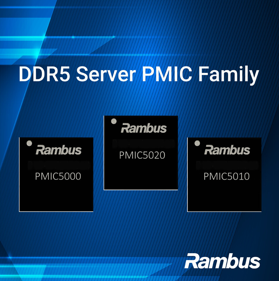
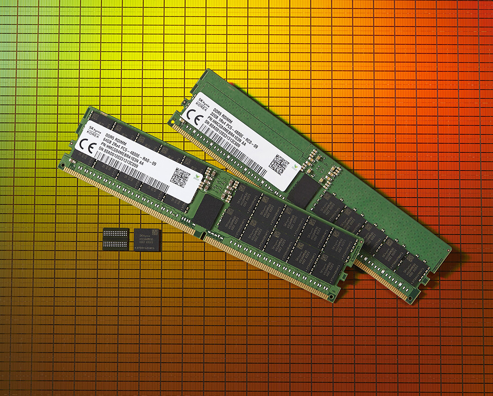
Rambus Inc., a premier chip and silicon IP provider making data faster and safer, today announced the availability of complete client chipsets for next-generation AI PC memory modules, featuring two new Power Management ICs (PMICs) for client computing. PMICs are critical to efficiently power memory modules providing breakthrough levels of performance for advanced computing applications. The two new Rambus industry-leading PMICs are the PMIC5200, for LPDDR5 CAMM2 (LPCAMM2) memory modules and the PMIC5120, which supports DDR5 CSODIMMs and CUDIMMs.
These PMICs, alongside the Client Clock Driver (CKD) and Serial Presence Detect Hub (SPD Hub), comprise a complete chipset offering to enable memory modules for AI PC notebooks, desktops and workstations. Further, with the addition of these new PMICs, Rambus now offers complete memory interface chipsets for all JEDEC standard DDR5 and LPDDR5 memory modules for both servers and clients.

These PMICs, alongside the Client Clock Driver (CKD) and Serial Presence Detect Hub (SPD Hub), comprise a complete chipset offering to enable memory modules for AI PC notebooks, desktops and workstations. Further, with the addition of these new PMICs, Rambus now offers complete memory interface chipsets for all JEDEC standard DDR5 and LPDDR5 memory modules for both servers and clients.