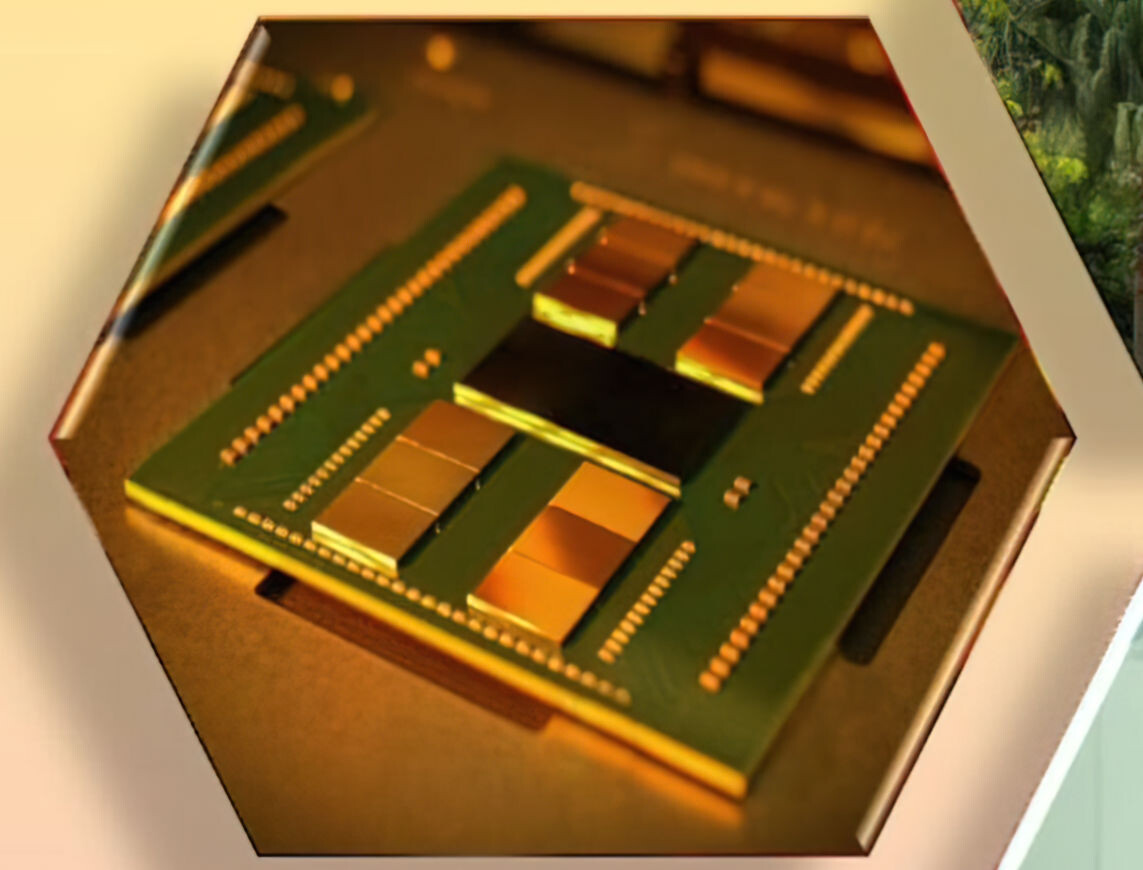
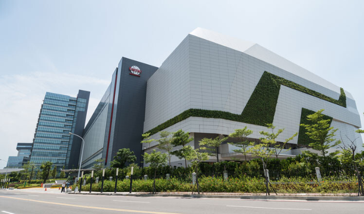
Huawei Obtained Two Million Ascend 910B Dies from TSMC via Shell Companies to Circumvent US Sanctions
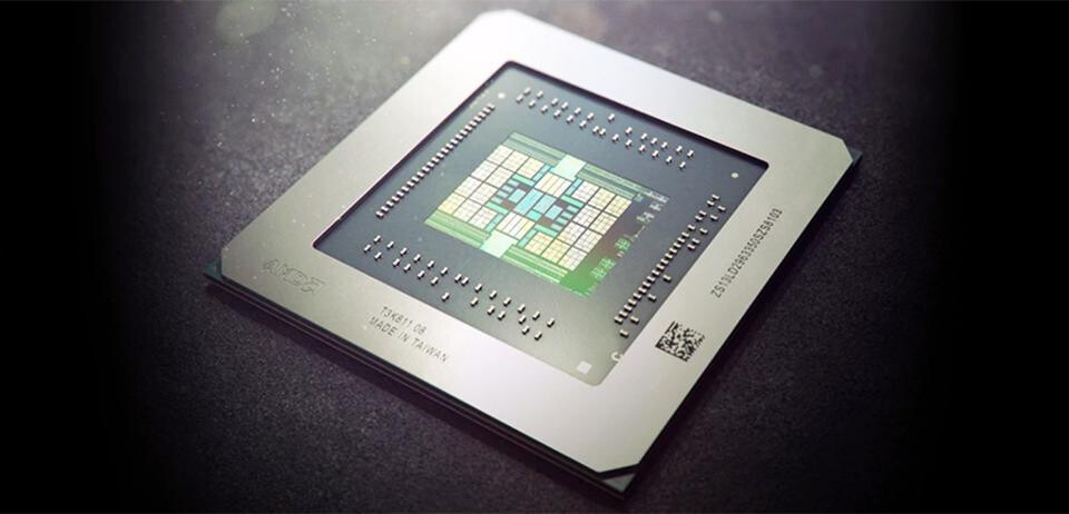
According to a recent Center for Strategic and International Studies report, Huawei got its hand on approximately two million Ascend 910B logic dies through shell companies that misled TSMC. This acquisition violates US export controls designed to restrict China's access to advanced semiconductor technology. The report details how Huawei leveraged intermediaries to procure chiplets for its AI accelerators before TSMC discovered the deception and halted shipments. These components are critical for Huawei's AI hardware roadmap, which progressed from the original Ascend 910 (manufactured by TSMC on N7+ until 2020) to the domestically produced Ascend 910B and 910C chips fabricated at SMIC using first and second-generation 7 nm-class technologies, respectively. Huawei reportedly wanted TSMC-made dies because of manufacturing challenges in domestic chip production. The Ascend 910B and 910C reportedly suffer from poor yields, with approximately 25% of units failing during the advanced packaging process that combines compute dies with HBM memory.
Despite these challenges, the performance gap with market-leading solutions still remains but has narrowed considerably, with the Ascend 910C reportedly delivering 60% of NVIDIA H100's performance. Huawei has executed a strategic stockpiling initiative, particularly for high-bandwidth memory components. The company likely acquired substantial HBM inventory between August and December 2024, when restrictions on advanced memory sales to China were announced but not yet implemented. The semiconductor supply chain breach shows that enforcing technology export controls is challenging, and third parties can still purchase silicon for restricted companies. While Huawei continues building AI infrastructure for both internal projects and external customers, manufacturing constraints may limit its ability to scale deployments against competitors with access to more advanced manufacturing processes. Perhaps a future domestic EUV-based silicon manufacturing flow will allow Huawei to gain access to more advanced domestic production, completely circumventing US-imposed restrictions.
Despite these challenges, the performance gap with market-leading solutions still remains but has narrowed considerably, with the Ascend 910C reportedly delivering 60% of NVIDIA H100's performance. Huawei has executed a strategic stockpiling initiative, particularly for high-bandwidth memory components. The company likely acquired substantial HBM inventory between August and December 2024, when restrictions on advanced memory sales to China were announced but not yet implemented. The semiconductor supply chain breach shows that enforcing technology export controls is challenging, and third parties can still purchase silicon for restricted companies. While Huawei continues building AI infrastructure for both internal projects and external customers, manufacturing constraints may limit its ability to scale deployments against competitors with access to more advanced manufacturing processes. Perhaps a future domestic EUV-based silicon manufacturing flow will allow Huawei to gain access to more advanced domestic production, completely circumventing US-imposed restrictions.