News Posts matching #Transistor

Return to Keyword Browsing

GK104 Transistor Count and Exact Die-Size Revealed

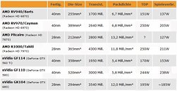
A part of the reason why NVIDIA's performance-segment GK104 is gunning for the performance crown from AMD's Tahiti GPU could be hidden behind two of its key specifications: transistor count, and die-size. 3DCenter.org compiled these two specifications for the GK104 from reliable sources, which pin the transistor count at 3.54 billion, and die-area at 294 mm². This yields a transistor density of 12 million per mm², which is slightly higher than that of AMD Tahiti, slightly lower than that of AMD Pitcairn, and certainly higher than previous-generation chips from both AMD and NVIDIA. If GeForce GTX 680 does in fact end up competitive with AMD's Radeon HD 7900 series, it could serve as a tell-tale sign of NVIDIA's Kepler architecture being a more efficient one.

Scientists Invent First Functional Single-Atom Transistor

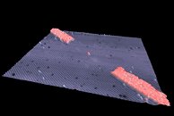
A team of scientists at the ARC Centre for Quantum Computation and Communication, at the University of New South Wales (UNSW), unveiled a fully functional single-atom transistor, which they predict will go on to become a critical building block of tomorrow's high-performance computing devices. The new transistor design was described in a paper, published by Nature. The active component of this transistor is a single phosphorous atom patterned between atomic-scale electrodes and control gates.

Single atom transistor designs have been attempted in the past, but those designs have had an error of about 10 nanometres in positioning of the atoms, which is big enough to affect their functionality. Professor Michelle Simmons, group leader of this study, said that this is the first time "anyone has shown control of a single atom in a substrate with this level of precise accuracy," adding that "Several groups have tried this, but if you want to make a practical computer in the long-term you need to be able to put lots of individual atoms in."

A video presentation by the group follows.

IBM Creates 9 nm Transistors Using Carbon Nanotubules

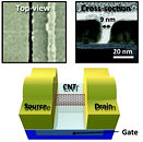
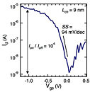
Researchers at IBM have developed the smallest carbon nanotubule transistor, that is 9 nanometers (nm) across. In comparison, the smallest transistors possible using silicon is 10 nm across. IBM claims its new transistor consumes less power while being able to carry more current than today's technology.

"The results really highlight the value of nanotubes in the most sophisticated type of transistors," says John Rogers, professor of materials science at the University of Illinois at Urbana-Champaign. "They suggest, very clearly, that nanotubes have the potential for doing something truly competitive with, or complementary to, silicon." Currently, the smallest production-grade transistors are 22 nm across.

AMD Realizes That Bulldozer Has 800 Million LESS Transistors Than It Thought!

AMD's new flagship Bulldozer "FX" series of processors have turned out to be mediocre performers in almost every review and benchmark going, sometimes even getting bested by the existing Phenom II and certainly no match for their Intel competition. To add to this tale of fail, it now turns out that AMD didn't even know how many transistors they have! Anand Lal Shimpi of AnandTech received an email from AMD's PR department and this is the revelation he had to share with us:
This is a bit unusual. I got an email from AMD PR this week asking me to correct the Bulldozer transistor count in our Sandy Bridge E review. The incorrect number, provided to me (and other reviewers) by AMD PR around 3 months ago was 2 billion transistors. The actual transistor count for Bulldozer is apparently 1.2 billion transistors. I don't have an explanation as to why the original number was wrong, just that the new number has been triple checked by my contact and is indeed right. The total die area for a 4-module/8-core Bulldozer remains correct at 315 mm².

Ivy Bridge Official Benchmarks - Markedly Better Performance Than Sandy Bridge

Previous preliminary reports have suggested that the forthcoming Ivy Bridge CPUs will have single threaded performance on par with the existing Sandy Bridge CPUs and will mainly deliver improvements to power consumption and integrated graphics - nothing for PC enthusiasts to get excited about. However, in leaked documents sent to partners, Intel have now revealed official performance figures for IB and they look rather good. They've produced a raft of benchmarks, which reveal improvements such as 56% in ArcSoft Media Expresso, 25% in Excel 2010 and a 199% gain in the 3D Mark Vantage GPU benchmark. Unfortunately, they haven't released any benchmarks based on high performance 3D games, but it's probably safe to say that they will be similarly improved. Now, on to the benchmarks, which compare their new 3.4 GHz i7-3770 (4 cores + HT) with the current 3.4 GHz i7-2600, also with 4 cores + HT:

Intel Reinvents Transistors Using New 3-D Structure

Intel Corporation today announced a significant breakthrough in the evolution of the transistor, the microscopic building block of modern electronics. For the first time since the invention of silicon transistors over 50 years ago, transistors using a three-dimensional structure will be put into high-volume manufacturing. Intel will introduce a revolutionary 3-D transistor design called Tri-Gate, first disclosed by Intel in 2002, into high-volume manufacturing at the 22-nanometer (nm) node in an Intel chip codenamed "Ivy Bridge." A nanometer is one-billionth of a meter.

The three-dimensional Tri-Gate transistors represent a fundamental departure from the two-dimensional planar transistor structure that has powered not only all computers, mobile phones and consumer electronics to-date, but also the electronic controls within cars, spacecraft, household appliances, medical devices and virtually thousands of other everyday devices for decades.

Intel Finds a New Material to Make Transistors, Tries for Cooler Processors

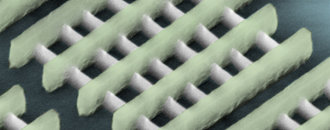
A quick and brief report on Innovation@Intel claims that the company's engineers have discovered a way to make transistors using new silicon substrate and thus reduce the heat and voltage output of future processors. The new transistors run far cooler - at about ½ the voltage, consuming only 1/10th the power of today's transistors.
Intel recently disclosed advancement details on a P-channel transistor, built on a silicon substrate, that makes use of compound semiconductors, also known as III-V materials because they are made of elements that straddle silicon in the periodic table, silicon being in column IV. This research resulted in the highest performing P-channel transistors reported to date. A year earlier, Intel described III-V N-channel transistors, also built on a silicon substrate. When combined, these two results could form the building blocks for CMOS logic circuits, which use both N-channel and P-channel transistors. Potentially suitable for future microprocessors, they run far cooler - at about ½ the voltage, consuming only 1/10th the power of today's transistors.

Intel Marks 60th Anniversary of the Transistor

Intel Corporation on Dec. 16 celebrates the 60th anniversary of the transistor, the building block of today's digital world. Invented by Bell Labs and considered one of the most important inventions of the 20th century, transistors are found in many consumer electronics and are the fundamental component used to build computer chips, or the "brains" of the personal computer (PC).
Return to Keyword Browsing
Dec 17th, 2024 20:45 EST change timezone

New Forum Posts

Popular Reviews

Controversial News Posts