News Posts matching #Vega

Return to Keyword Browsing

Sony Closely Associated with AMD "Navi" Development

AMD monetizes its GPU IP not just with discrete graphics cards and integrated graphics in its PC processors, but also by selling semi-custom SoCs for most modern game consoles, such as the Xbox One and PlayStation 4, with some of the newer 4K UHD-capable models such as the PlayStation 4 Pro and Xbox One X even leveraging newer graphics architectures by the company, such as "Polaris." 2020 could see the roll out of next-generation gaming consoles, which are more purpose-built for 4K UHD gaming, with visual fidelity matching gaming PCs, and so console manufacturers are looking for a lean and powerful new GPU IP. Sony seems to have made up its mind of sticking with AMD.

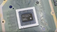
AMD will supply a semi-custom SoC to Sony for its next major console, "PlayStation 5." This chip will feature a graphics processor based on the "Navi" architecture, which succeeds "Vega." 2020 could also be the year when the 7 nm silicon fabrication process achieves some maturity and makes up most of the bulk ASIC production nodes. According to Tweaktown, Sony is closely working with AMD for the development of the "Navi" architecture itself, so versions of it are efficient enough to be deployed in console SoCs that are built to a cost. The design goal will be to enable 4K @ 60 Hz gaming, as 4K televisions will have proliferated a lot by 2020.
AMD "Vega" Outsells "Previous Generation" by Over 10 Times

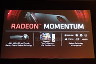
At its Computex presser, leading up to its 7 nm Radeon Vega series unveil, AMD touched upon the massive proliferation of the Vega graphics architecture, which is found not only in discrete GPUs, but also APUs, and semi-custom SoCs of the latest generation 4K-capable game consoles. One such slide that created quite some flutter reads that "Vega" shipments are over 10 times greater than those of the "previous generation."

Normally you'd assume the previous-generation of "Vega" to be "Polaris," since we're talking about the architecture, and not an implementation of it (eg: "Vega 10" or "Raven Ridge," etc.). AMD later, at its post event round-table, clarified that it was referring to "Fiji," or the chip that went into building the Radeon R9 Fury X, R9 Nano, etc., and comparing its sales with that of products based on the "Vega 10" silicon. Growth in shipments of "Vega" based graphics cards is triggered by the crypto-mining industry, and for all intents and purposes, AMD considers the "Vega 10" silicon to be a commercial success.

AMD Demonstrates 7nm Radeon Vega Instinct HPC Accelerator

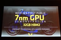
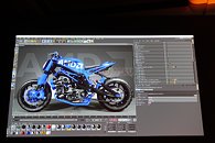
AMD demonstrated the world's first GPU built on the 7 nanometer silicon fabrication process, a Radeon Vega Instinct HPC/AI accelerator, with a 7 nm GPU based on the "Vega" architecture, at its heart. This chip is an MCM of a 7 nm GPU die, and 32 GB HBM2 memory stacks over four stacks (4096-bit memory bus width). It's also the first product to feature a removable InfinityFabric interface (competition to NVIDIA's NVLink interface). There will also be variants based on the common PCI-Express 3.0 x16. The card supports hardware virtualization and new deep-learning ops.

AMD Readies Athlon 200GE and Athlon Pro 200GE: First Athlon Branded "Zen"

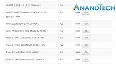
AMD is giving finishing touches to the Athlon 200GE (YD200GC6M2OFB) and Athlon Pro 200GE (YD200GC6M20FB) socket AM4 APUs, which will likely be a part of the company's answer to Intel's Pentium Gold series. The "E" brand extension denotes energy-efficiency, and both chips have a rated TDP of just 35W. The two are based on AMD's 14 nm "Raven Ridge" silicon, and pack a 2-core/4-thread CPU based on the "Zen" microarchitecture, clocked at 3.20 GHz.

Unlike previous few generations of Athlon-branded parts, which were essentially socket FM2(+) APUs devoid of integrated graphics, the Athlon 200GE and Athlon Pro 200GE do feature the Radeon Vega integrated graphics solution, but we expect it to be watered down compared to the Ryzen 2000G series chips. What sets the Athlon Pro part apart from its non-Pro sibling is the same feature that set Ryzen Pro apart, such as SEV. The two chips surfaced on the updated CPU compatibility lists of ASUS Crosshair VII Hero X470.

AMD Introduces Broad AMD Ryzen PRO Mobile & Desktop APU Systems for Enterprise

AMD today announced unprecedented adoption of its AMD Ryzen PRO processors - including new notebooks and desktops powered by Ryzen PRO processors with built-in Radeon Vega graphics now available from the world's three largest enterprise PC OEMs. AMD Ryzen PRO APUs for premium commercial desktop and notebooks provide commercial PC buyers with new levels of choice and innovation and enable Dell, HP, and Lenovo to create a range of business systems, from sleek enterprise notebooks to powerful commercial desktops. Combined, these systems make up the broadest portfolio of AMD processor-based enterprise PCs in the company's history.

AMD "Vega 20" with 32 GB HBM2 3DMark 11 Score Surfaces

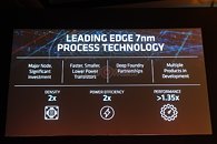
With the latest Radeon Vega Instinct reveal, it's becoming increasingly clear that "Vega 20" is an optical shrink of the "Vega 10" GPU die to the new 7 nm silicon fabrication process, which could significantly lower power-draw, enabling AMD to increase clock-speeds. A prototype graphics card based on "Vega 20," armed with a whopping 32 GB of HBM2 memory, was put through 3DMark 11, on a machine powered by a Ryzen 7 1700 processor, and compared with a Radeon Vega Frontier Edition.

The prototype had lower GPU clock-speeds than the Vega Frontier Edition, at 1.00 GHz, vs. up to 1.60 GHz of the Vega Frontier Edition. Its memory, however, was clocked higher, at 1250 MHz (640 GB/s) vs. 945 MHz (483 GB/s). Despite significantly lower GPU clocks, the supposed "Vega 20" prototype appears to score higher performance clock-for-clock, but loses out on overall performance, in all tests. This could mean "Vega 20" is not just an optical-shrink of "Vega 10," but also benefits from newer architecture features, besides faster memory.

AMD Teases Its 7 nm Vega Instinct Accelerator - Data-Pushing Silicon Deployed

AMD has announced via its Twitter feed that the Vega die shrink from current 14 nm down to 7 nm has actually coalesced into a hardware product that can be tested and vetted at their labs. Via a teaser image, the company said that "7nm @RadeonInstinct product for machine learning is running in our labs."

Of course, working silicon is only half the battle - considerations such as yields, leakage, and others are all demons that must be worked out for actual production silicon, which may thus be some months off. Only AMD and TSMC themselves themselves know how the actual production run went - and the performance and power efficiency that can be expected from this design (remember that AMD's CEO Lisa SU herself said they'd partner with both TSMC and Globalfoundries for the 7 nm push, though it seems TSMC may be pulling ahead in that field). Considering AMD's timeline for the die-shrunk Vega to 7 nm - with predicted product launch for 2H 2018 - the fact that there is working silicon being sampled right now is definitely good news.
Return to Keyword Browsing
Dec 18th, 2024 00:39 EST change timezone

New Forum Posts

Popular Reviews

Controversial News Posts