News Posts matching #vega 20

Return to Keyword Browsing

TechPowerUp GPU-Z v2.26.0 Released

Today we released the latest version of TechPowerUp GPU-Z, the popular graphics subsystem information, monitoring, and diagnostic utility. Version 2.26.0 adds support for new GPUs, introduces new features, and fixes problems with existing ones. To begin with, support is added for AMD Radeon RX 5500 and RX 5500M, TU104-based NVIDIA GeForce RTX 2060 (non-Super), and Quadro P520. Fake detection has been added for various "Kepler" based GTX 10-series knockoffs.

With this release we fixed an application crash during BIOS extraction on nearly all NVIDIA GPUs. Another crash that appears when the application is launched on machines with AMD "Navi" GPUs without drivers installed. The ASUS ROG skin has been fixed to properly show the "Close" button in the bottom. We also improved the memory junction temperature tooltip on AMD "Navi" to denote that the hottest chip's junction temperature is being reported, and not an average across all chips. Last version's AMD Navi fan-stop fix has been reverted since AMD fixed the issue since their 19.9.1 drivers. PCIe and CrossFire state detection has been fixed for AMD "Navi" and "Vega 20" based graphics cards. Grab it from the link below.

DOWNLOAD: TechPowerUp GPU-Z v2.26.0
The change-log follows.

Radeon VII Lacks Full FP64 Compute Capabilities Available to Instinct MI60

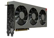
AMD's upcoming Radeon VII high-end consumer graphics card lacks full FP64 compute capabilities available to the company's other products targeting the enterprise-compute market, such as the Radeon Instinct MI60. Radeon VII offers an FP32 peak compute throughput of 13.8 TFLOP/s single-precision, which, given its hardware resources, should normally work out a double-precision throughput of 6.7 TFLOP/s. However, with the feature disabled for the Radeon VII, the FP64 throughput will be closer to 860 GFLOP/s. Disabling FP64 capabilities for client-segment graphics cards is a common practice among both AMD and NVIDIA.

For gamers, PC enthusiasts, and even creative professionals, double-precision floating-point performance of a graphics card remains completely irrelevant. The disabling of DPFP ensures gamers have access to Radeon VII, lest every cloud compute provider and their dog would soak up Radeon VII inventory owing to its $699 list price, had it offered 6.7 TFLOP/s rivaling compute accelerators 10-15 times more. Radeon VII is the world's first consumer graphics processor built on the 7 nm silicon fabrication process, with company-claimed performance rivaling NVIDIA's RTX 2080. It will be available from February 7.

Vega II Logo Trademarked by AMD

AMD late November filed a trademark application with the USPTO for a new logo, for its second generation "Vega" graphics architecture, built around the 7 nm silicon fabrication process. The logo looks similar to the original Vega "V," with two bands marking out the Roman numeral II (2). This logo could appear on the product and marketing on a series of new Radeon Pro and Radeon Instinct (and possibly even gaming-grade Radeon RX?) graphics cards based on AMD's new "Vega 20" multi-chip module. This chip features a doubling in memory bandwidth thanks to its 4096-bit wide HBM2 interface, and the optical shrink of the GPU die to the 7 nm node could enable AMD to dial up engine clocks significantly.

AMD "Vega 20" GPU Not Before Late Q1-2019

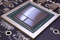
AMD "Vega 20" is a new GPU based on existing "Vega" graphics architecture, which will be fabbed on the 7 nanometer silicon fabrication process, and bolstered with up to 32 GB of HBM2 memory across a 4096-bit memory interface that's double the bus-width of "Vega 10". AMD CEO Lisa Su already exhibited a mock-up of this chip at Computex 2018, with an word that alongside its "Zen 2" based EPYC enterprise processors, "Vega 20" will be the first 7 nm GPU. AMD could still make good on that word, only don't expect to find one under your tree this Holiday.

According to GamersNexus, the first "Vega 20" products won't launch before the turn of the year, and even in 2019, one can expect product launches till the end of Q1 (before April). GamersNexus cites reliable sources hinting at the later-than-expected arrival of "Vega 20" as part of refuting alleged "Final Fantasy XV" benchmarks of purported "Vega 20" engineering samples doing rounds on the web. Lisa Su stressed the importance of data-center GPUs in AMD's Q3-2018 earnings call, which could hint at the possibility of AMD allocating its first "Vega 20" yields to high-margin enterprise brands such as Radeon Pro and Radeon Instinct.

AMD Radeon Vega 12 and Vega 20 Listed in Ashes Of The Singularity Database

Back at Computex, AMD showed a demo of their Vega 20 graphics processor, which is produced using a refined 7 nanometer process. We also reported that the chip has a twice-as-wide memory interface, effectively doubling memory bandwidth, and alsomaximum memory capacity. The smaller process promises improvements to power efficiency, which could let AMD run the chip at higher frequencies for more performance compared to the 14 nanometer process of existing Vega.

As indicated by AMD during Computex, the 7 nanometer Vega is a product targeted at High Performance Compute (HPC) applications, with no plans to release it for gaming. As they clarified later, the promise of "7 nanometer for gamers" is for Navi, which follows the Vega architecture. It's even more surprising to see AOTS results for a non-gaming card - my guess is that someone was curious how well it would do in gaming.

AMD "Vega 20" with 32 GB HBM2 3DMark 11 Score Surfaces

With the latest Radeon Vega Instinct reveal, it's becoming increasingly clear that "Vega 20" is an optical shrink of the "Vega 10" GPU die to the new 7 nm silicon fabrication process, which could significantly lower power-draw, enabling AMD to increase clock-speeds. A prototype graphics card based on "Vega 20," armed with a whopping 32 GB of HBM2 memory, was put through 3DMark 11, on a machine powered by a Ryzen 7 1700 processor, and compared with a Radeon Vega Frontier Edition.

The prototype had lower GPU clock-speeds than the Vega Frontier Edition, at 1.00 GHz, vs. up to 1.60 GHz of the Vega Frontier Edition. Its memory, however, was clocked higher, at 1250 MHz (640 GB/s) vs. 945 MHz (483 GB/s). Despite significantly lower GPU clocks, the supposed "Vega 20" prototype appears to score higher performance clock-for-clock, but loses out on overall performance, in all tests. This could mean "Vega 20" is not just an optical-shrink of "Vega 10," but also benefits from newer architecture features, besides faster memory.

AMD To Change Suppliers for Vega 20 GPUs on 7nm, HBM2 Packaging for Vega 11

AMD's RX Vega supply has seen exceedingly limited quantities available since launch. This has been due to a number of reasons, though the two foremost that have been reported are: increased demand from cryptocurrency miners, who are looking towards maximizing their single node hashrate density through Vega's promising mining capabilities; and yield issues with AMD's Vega 10 HBM2 packaging partner, Advanced Semiconductor Engineering (ASE). It's expected that chip yield for Vega 10 is also lower per se, due to it having a 484 mm² die, which is more prone to defects than a smaller one, thus reducing the amount of fully-enabled GPUs.

AMD's production partner, GlobalFoundries, has historically been at the center of considerations on AMD's yield problems. That GlobalFoundries is seemingly doing a good job with Ryzen may not be much to say: those chips have incredibly small die sizes (192 mm²) for their number of cores. It seems that Global Foundries only hits problems with increased die sizes and complexity (which is, unfortunately for AMD, where it matters most).
Return to Keyword Browsing
Jan 18th, 2025 00:11 EST change timezone

New Forum Posts

Popular Reviews

Controversial News Posts